
<h2>I. Event Recap: Intel Secures First High-NA EUV Mass Production Rights</h2>
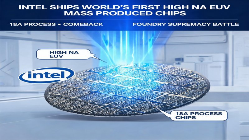
<p>On July 15, 2026, ASML and Intel jointly released an announcement capable of rewriting the global semiconductor industry landscape: Intel Foundry, based on its 18A process node, successfully mass-produced Intel Core Ultra Series 3 processors (codenamed Panther Lake) using ASML's EXE:5000 High NA EUV lithography systems, becoming the world's first chipmaker to deploy High NA EUV technology in high-volume logic chip production. The significance of this milestone cannot be overstated—High NA EUV is regarded by the industry as the 'final trump card' for extending Moore's Law, with each machine costing approximately $400 million (about 2.7 billion RMB), and only Dutch company ASML capable of production globally.</p>
<p>According to ASML's official disclosure, Intel used High NA EUV equipment at its Oregon factory to lithograph specific critical layers of the Panther Lake processors. These chips are based on Intel's most advanced 18A process (equivalent to 1.8nm class), employing two core technologies: RibbonFET gate-all-around transistors (GAA) and PowerVia backside power delivery network. Notably, Intel is currently using High NA EUV only on select critical layers rather than all layers, indicating the technology remains in early mass production stages, but is already sufficient to prove its reliability and economics in a production environment.</p>
<p>Financially, Intel's Q1 2026 earnings showed Non-GAAP gross margin reaching 41%, exceeding guidance by approximately 650 basis points, partly benefiting from 18A process yield improvements. The company's Q2 revenue guidance is $13.8-14.8 billion, representing 2-9% quarter-over-quarter growth. CEO Lip-Bu Tan stated in the earnings call that server CPU demand expectations have significantly improved over the past 90 days, with full-year 2026 industry and Intel unit growth both expected to reach double digits. Meanwhile, ASML raised its 2026 guidance on the same day as the announcement, explicitly citing Intel's High NA EUV mass production as one of the key drivers.</p>
<h2>II. Technical Depth: From 0.33 to 0.55, How High NA EUV Reshapes Transistor Scaling</h2>
<p>To understand the High NA EUV technical breakthrough, one must return to the fundamental physics of lithography. Numerical Aperture (NA) is the core parameter determining lithography system resolution, with the formula R = k1 * λ / NA, where R is resolution, λ is light source wavelength, and k1 is the process factor. ASML's previous-generation NXE series EUV lithography machines had an NA of 0.33, using 13.5nm wavelength extreme ultraviolet light, with theoretical resolution of about 13nm. The new EXE:5000 increases NA to 0.55, compressing theoretical resolution to 8nm at the same wavelength—an improvement of 1.7x. The direct effect of this advance is that chip manufacturers can print finer transistor features with single-patterning rather than multi-patterning as in the past, significantly reducing process steps, shortening production cycles, and improving yield.</p>
<p>Intel's 18A process is among the first beneficiaries of this technological dividend. According to technical papers disclosed at the VLSI Symposium in June 2026, the 18A process achieves the following key parameters at the standard cell level: transistor density of approximately 220 million per square millimeter (comparable to TSMC N2), RibbonFET nanosheet width as low as 3nm, and PowerVia backside power delivery reducing signal routing resistance by approximately 30%. More critically, Intel developed an enhanced 18A-P (18A-Performance) based on 18A, delivering over 9% performance improvement at iso-power, or over 18% power reduction at iso-performance. These parameters mean 18A-P already possesses the capability to compete head-to-head with TSMC N2 on comprehensive power-performance-area (PPA) metrics.</p>
<p>The physical realization of High NA EUV is not simply a parameter upgrade but a bet on precision optical engineering. To increase NA from 0.33 to 0.55, ASML engineers had to increase the primary mirror diameter in the optical system by approximately 50%, causing the light incidence angle on the reticle to increase significantly. Larger incidence angles reduce reticle reflectivity, so ASML developed new 'high-absorptance multilayer film' reticle technology and redesigned the reticle geometry (from traditional 6-inch×6-inch to 'anamorphic' design). Additionally, higher NA means shallower depth of focus, imposing stricter requirements on wafer flatness and process window control. These engineering challenges made the R&D and manufacturing cycle for High NA EUV equipment span over a decade, also explaining why each machine costs $400 million—nearly double the price of standard EUV equipment (approximately $200 million).</p>
<p>From an industry impact perspective, High NA EUV mass production will usher chip manufacturing into the '8nm resolution era,' sufficient to support at least two process generations (18A and future 14A) with single-patterning. Intel plans to use High NA EUV on select critical layers of 18A (primarily logic transistor fins and gates layers), while continuing to use standard EUV or DUV for interconnect layers. This 'hybrid strategy' controls capital expenditure while maintaining technological leadership. Industry estimates suggest that a fab producing 50,000 wafers per month at 18A, if using High NA EUV on all layers, would require equipment investment exceeding $15 billion; Intel's 'selective adoption' strategy may keep this figure in the $8-10 billion range.</p>
<h2>III. Financial Logic: Intel Foundry's Path to Profitability and the Hundred-Billion-Dollar Bet</h2>
<p>Intel's investment in High NA EUV and the 18A process is the core component of CEO Pat Gelsinger's 'IDM 2.0' strategy since taking office in 2021, and also a financial bet involving hundreds of billions of dollars. Intel plans to advance five process nodes in four years (Intel 7, Intel 4, Intel 3, Intel 20A, Intel 18A) and build or expand fabs globally, including Arizona, Oregon, New Mexico in the US, and Magdeburg in Germany and Ireland in Europe. External estimates suggest Intel's wafer manufacturing capital expenditure from 2022-2026 exceeds $90 billion, with a substantial portion flowing to ASML EUV and High NA EUV equipment purchases.</p>
<p>From a financial return perspective, the yield improvement of the 18A process is the key variable determining whether Intel Foundry can turn profitable. According to recent industry reports, Intel 18A process yield has jumped from 65% last quarter to 85%—a leap rarely seen in advanced process history. For comparison, TSMC N3 (3nm) had initial mass production yields of approximately 60-70%, improving to over 80% after about 18 months of optimization. The rapid improvement in Intel 18A yield owes partly to High NA EUV's systematic advantage of reducing process steps, and partly to the release of Intel's technical accumulation in process integration and defect control.</p>
<p>Customer order progress further validates 18A's commercial viability. In addition to Intel's own products (Panther Lake, Nova Lake), Apple has been rumored in the market as an early external customer for 18A/18A-P, with future M-series chips potentially partially or fully using Intel foundry services. More explosively, industry rumors suggest AMD and NVIDIA are also evaluating Intel's 18A process—if these two largest fabless chip design companies allocate partial capacity of their flagship products (such as AMD EPYC, NVIDIA AI accelerators) to Intel, it would completely reshape the global foundry customer landscape. From unit economics, an 18A-process 12-inch wafer foundry price is estimated at $18,000-22,000; if Intel Foundry can achieve monthly production of 100,000 18A wafers in 2027, annual revenue contribution will exceed $20 billion, sufficient to cover its massive depreciation costs and achieve profitability.</p>
<p>However, Intel's financial pressure remains enormous. Although Q1 2026 Non-GAAP gross margin exceeded expectations at 41%, the company remains loss-making on a GAAP basis. The foundry business's massive capital expenditure continues to drag on free cash flow, forcing Intel in 2025 to improve its balance sheet through partial Altera equity sale and 15% workforce reduction. While High NA EUV equipment purchases have won Intel technological leadership, they also mean additional quarterly depreciation amortization pressure. The financial metric investors need to watch closely is when Intel Foundry business can achieve quarterly operating profit turnaround. Management guidance implies this goal may be reached between Q4 2026 and H1 2027, contingent on 18A external customer orders meeting expectations and yields stabilizing above 85%.</p>
<h2>IV. Strategic Depth: The Restructuring of Intel, TSMC, and Samsung's Three-Way Battle</h2>
<p>The success of Intel's High NA EUV mass production is breaking the foundry landscape of the past five years where 'TSMC dominated, Samsung chased, and Intel lagged,' pushing the industry into a new stage of 'three-strong错位 competition.' The following matrix compares the current state of the three companies in advanced processes across multiple dimensions:</p>
| Dimension | Intel (18A) | TSMC (N2/A16) | Samsung (SF2/SF3) |
|---|---|---|---|
| Mass Production Node | 18A (2026 mass production) | N2 (H2 2025 mass production) | SF3 (2024 mass production), SF2 (H2 2026) |
| High NA EUV | In mass production (world's first) | Planned 2029 deployment | Planned 2027-2028 evaluation |
| Transistor Architecture | RibbonFET GAA + PowerVia backside power | GAA (N2) + traditional power | GAA (from 3nm) |
| Disclosed Yield | 85% (18A) | Not disclosed (estimated 80-85%) | Relatively low (rumored 50-60%) |
| Q2 2026 Revenue | Guidance $13.8-14.8 billion | ~$40.2 billion (NT$1,270.4B) | Semiconductor division under pressure, stock -8.8% |
| Q2 Net Profit Margin | GAAP still loss-making | 55.6% net margin | Sharp decline |
| Major External Customers | Apple (rumored), own products | Apple, NVIDIA, AMD, Qualcomm | Qualcomm (partial), own products |
| Geopolitical Risk | Low (US本土+Europe layout) | High (Taiwan Strait risk concentration) | Medium (Korea本土+US fab construction) |
<p>From the table above, the strategic错位 of the three companies is clearly visible. TSMC's advantages lie in scale, customer ecosystem, and profitability—Q2 revenue of $40.2 billion and 55.6% net profit margin financial performance is practically 'money-printing machine' level, with top customers like Apple, NVIDIA, and AMD forming an immeasurably deep moat. However, TSMC's conservative stance on High NA EUV (planned 2029 deployment) may expose it to technological generation-gap risks during 2026-2028, particularly when Intel 18A-P's PPA metrics are validated by customers, and some performance-extremely-sensitive customers (such as AI chip companies) may be willing to undertake supply chain risks in exchange for process advantages.</p>
<p>Samsung's situation is the most difficult. Although its 3nm GAA process is theoretically equivalent to TSMC N3, actual yield has been chronically low (rumored in the 50-60% range), causing core customers like Qualcomm to shift orders back to TSMC. Samsung's stock plummeted 8.8% on July 16, 2026, reflecting market deep concerns about its semiconductor business competitiveness. Samsung's plans for High NA EUV are even more vague, with evaluation expected only in 2027-2028, meaning it cannot compete head-to-head with Intel in advanced processes until at least 2028. Samsung's only way out may be to defend the mid-to-low-end market through price wars while hoping for progress at its new Taylor, Texas facility.</p>
<p>Intel's strategic opportunity window lies in the dual叠加 of 'technological leadership + geopolitical红利.' With subsidy support from the US CHIPS Act, Intel's US domestic manufacturing capability becomes a unique advantage for securing US government and defense orders. Meanwhile, global tech giants' concerns about 'Taiwan Strait risks' are growing, with unprecedented willingness to diversify supply chains. If Intel can prove 18A process reliability and capacity scale during 2026-2027, it will have the opportunity to divert some high-end orders from TSMC and reshape the position of 'Made in USA' in advanced semiconductors.</p>
<h2>V. Challenges and Concerns: Yield Sustainability, Customer Trust, and Capital Returns</h2>
<p>Although news of Intel's High NA EUV mass production and 18A yield improvements is exciting,冷静 analysis of its risks is equally necessary. The primary challenge is yield sustainability. While 85% yield has reached mass-production viability, it still lags TSMC N3's mature yield of 90%+. More importantly, this yield data is currently based only on Intel's own product (Panther Lake) production; external customers (such as Apple) may have design rules, IP libraries, and physical layouts differing from Intel's own products, potentially causing yield '水土不服' during new customer ramp-ups. Historically, Intel suffered from yield ramping far slower than expected at both 14nm and 10nm nodes; whether 18A can avoid repeating these mistakes requires at least two quarters of sustained data validation.</p>
<p>The second major challenge is rebuilding customer trust. Before 2021, Intel Foundry business had almost no experience serving external customers, and although its IFS (Intel Foundry Services) has signed some customers (such as MediaTek, Amazon AWS) since establishment, there has yet to be a true case of a 'top-tier chip design company entrusting flagship products to Intel foundry.' While Apple is rumored as an 18A customer, Apple is notoriously conservative in supply chain management, typically taping out at multiple foundries simultaneously to reduce risk, with initial capacity allocation to Intel likely very limited. Potential AMD and NVIDIA orders face even more complex technical and commercial evaluations—these two companies have cooperated with TSMC for over a decade, with design flows, EDA toolchains, and IP libraries deeply bound to TSMC processes, and migrating to Intel 18A requires massive upfront investment and at least 18-24 months of adaptation cycles.</p>
<p>The third risk is return on invested capital (ROIC) pressure. Intel's billions of dollars in capital expenditure for 18A and High NA EUV needs to be recovered through foundry revenue within the next 5-7 years. According to foundry industry experience, investment recovery periods for advanced process fabs typically range 6-8 years. If Intel Foundry cannot reach economies of scale above 100,000 wafers per month during 2027-2028, its unit costs will be significantly higher than TSMC's, falling into a 'high-price no-market' dilemma. Additionally, ASML High NA EUV equipment delivery cycles are 18-24 months, and ASML's capacity is limited (expected to deliver approximately 10-15 units in 2026), meaning even if Intel holds orders, it may be constrained by equipment arrival speed and unable to rapidly expand production.</p>
<p>Finally, the technology itself carries uncertainties. Although High NA EUV improves resolution to 8nm, its depth of focus is shallower than standard EUV, requiring higher wafer surface flatness. If in actual mass production, High NA EUV defect density exceeds expectations, longer process optimization cycles may be required. Additionally, Intel's planned PowerVia backside power delivery technology on 18A, while theoretically reducing resistance by 30%, may introduce new yield risks through its complex wafer bonding and thinning processes.</p>
<h2>VI. Conclusion: Investment and Procurement Decisions Amid Foundry Supremacy Restructuring</h2>
<p>Intel's shipment of the world's first High NA EUV mass-produced chip is the most symbolic technology milestone in the semiconductor industry in nearly five years. It not only proves Intel's technical execution under the 'IDM 2.0' strategy but also sends a clear signal to the market: in the ultimate race of advanced processes, Intel has transformed from follower back to leader. The triple technical breakthroughs of 18A process yield jumping from 65% to 85%, High NA EUV's first mass production, and 18A-P's further performance enhancement form a solid foundation for Intel Foundry business to turn losses into profits.</p>
<p>For chip design enterprise technology decision-makers, our recommendation is: immediately initiate Intel 18A process dual-source evaluation projects. Especially for AI inference chips, high-performance computing processors, and high-end FPGA products, 18A's PowerVia backside power delivery and RibbonFET architecture may offer superior power and performance compared to TSMC N2. We recommend completing the first tape-out before Q4 2026 to obtain mass production capacity by H2 2027. At the same time, do not completely abandon cooperation with TSMC—before Intel Foundry's capacity scale and customer support system fully mature, maintaining a 'TSMC-primary, Intel-secondary' dual-source strategy is the most prudent choice.</p>
<p>For enterprise supply chain and procurement leaders, it is necessary to reassess 2027-2028 foundry budgets and capacity allocation. Intel Foundry's rise will break TSMC's monopoly pricing power, and advanced process wafer prices are expected to face 5-10% downward pressure after 18A mass production. We recommend introducing Intel Foundry as an alternative option for price comparison in annual contract negotiations with TSMC,争取 more favorable prices and more flexible capacity allocation terms.</p>
<p>For tech investors, Intel's current valuation is at a historical low (price-to-book ratio approximately 1.5x), reflecting market pessimism about its foundry business's massive losses. High NA EUV mass production and 18A yield improvement are key catalysts to reverse this expectation. We recommend monitoring the following milestone events: (1) sequential growth rate of Foundry business revenue in Q3 2026 earnings; (2) official announcement of 18A external customers (beyond Apple); (3) progress toward achieving 80-90% self-production ratio for Nova Lake processors. If these events proceed as expected, Intel stock could achieve 30-50% revaluation within 12 months. Meanwhile, ASML, as the sole supplier of High NA EUV, will directly benefit from Intel's capacity expansion, and is recommended as a core holding in the semiconductor equipment sector.</p>
<p>Intel's success in High NA EUV mass production is like placing a 'tianyuan' (center point) piece on the foundry chessboard. It will not immediately end TSMC's dominance, but it certainly opens infinite possibilities for industry restructuring over the next three to five years. In this competition involving hundreds of billions of dollars in investment and determining the fate of global AI computing infrastructure, every technology node, every yield improvement, and every customer order will profoundly influence the final balance of victory.</p>
Why it Matters
High NA EUV is the 'holy grail' technology for next-generation semiconductor manufacturing, with each machine costing $400 million and only ASML capable of producing them globally. Intel's first-to-mass-production achievement means it has transformed from a 'follower' to a 'leader' in the advanced process race. This not only concerns the commercial success of Intel's own 18A process (yield has improved from 65% to 85%), but will also reshape the global foundry landscape—although TSMC's 2nm has entered mass production with profits surging 77.4%, it trails Intel by at least 3 years in the High NA EUV dimension; Samsung, meanwhile, saw its stock plummet 8.8% due to yield and capacity issues. For AI chip, smartphone, and HPC customers, this shift in process technology leadership will directly impact supply chain choices and cost structures.
DECISION
For chip design CTOs: Immediately initiate dual-source evaluation of Intel 18A process, especially for AI inference and HPC chips, as 18A's PowerVia backside power delivery and RibbonFET GAA architecture may offer better PPA than TSMC N2. For supply chain procurement leads: Renegotiate 2027-2028 foundry capacity allocation, as Intel Foundry's capacity release (Nova Lake self-production ratio increasing to 80-90%) will change the supply-demand landscape. For tech investors: Watch Intel's Q2 earnings for sequential changes in Foundry revenue and 18A customer expansion progress (Apple order confirmed, AMD/NVIDIA potential orders are key catalysts). For ASML shareholders: Intel's High NA EUV mass production confirmation supports ASML's 2026 guidance raise, recommend maintaining or increasing positions.
PREDICT
Q3 2026: Intel will announce at least 1-2 external 18A customers (beyond Apple), with AMD or NVIDIA adoption being key validation. Q4 2026: Intel 18A-P enters initial production, delivering 9% performance improvement or 18% power reduction over 18A, further narrowing the gap with TSMC N2. H1 2027: TSMC accelerates High NA EUV adoption plans, potentially moving the timeline from 2029 to 2028, triggering a surge in ASML orders. H2 2027: If Intel Foundry yields stabilize above 85% and capacity ramps smoothly, its global foundry market share could rise from under 10% to 15%, directly challenging Samsung for the #2 position.
Get 3-5 key AI infrastructure signals weekly →
💬 Comments (0)