
I. Event Recap
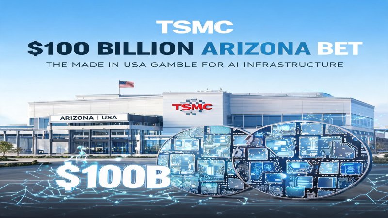
On July 16, 2026, TSMC, the world's leading foundry, reported its second quarter 2026 results, marking its fifth consecutive record quarter: revenue of $40.2 billion, up 33.7% year-over-year; net income up 77.4%; and gross margin reaching 67.7%, far exceeding industry averages. Beyond the stellar financial performance, TSMC CEO C.C. Wei announced a stunning investment plan: an additional $100 billion investment in Arizona, USA, for building 2nm and more advanced process fabs and advanced packaging facilities. This brings TSMC's total committed investment in Arizona to $265 billion.
TSMC also raised its 2026 full-year capital expenditure guidance to $60-64 billion and lifted Q3 revenue guidance to $44.6-45.8 billion. The company stated the additional investment aims to meet strong demand from major U.S. customers for years to come and support the development of the U.S. semiconductor ecosystem. However, markets reacted violently: on July 17, TSMC shares plunged 7.29%, and Taiwan's weighted index recorded its largest intraday drop in history, as investors deeply questioned the sustainability of AI capital expenditure.
The timing of this investment decision is significant. Just one day earlier (July 15), Dutch lithography giant ASML reported better-than-expected earnings and announced plans to raise prices for certain EUV and DUV equipment by approximately 10%. TSMC is resisting ASML's price hike, but ASML CFO Roger Dassen confirmed the company has stronger pricing power than in the past. TSMC's massive capex plan means it will continue purchasing large quantities of ASML equipment for years to come, and rising equipment costs will directly compress its gross margin space.
From a geopolitical strategic perspective, TSMC's Arizona investment also represents a response to the U.S. CHIPS and Science Act. This legislation attracts semiconductor manufacturing back to the U.S. through tax incentives and subsidies, but TSMC had previously been cautious about building advanced process fabs in America, with primary concerns including high costs, talent shortages, and cultural differences. This additional investment signals that under the dual drivers of geopolitical pressure and major customer demand, TSMC has incorporated 'Made in USA' into its core strategic layout.
II. Technical Depth
The technology roadmap for TSMC's Arizona fabs is key to understanding this investment. According to public information, the new facilities will focus on 2nm and more advanced processes, equipped with advanced packaging capabilities. The 2nm process is the next critical node for the semiconductor industry, adopting Gate-All-Around (GAA) transistor architecture to replace existing FinFET, enabling approximately 15% performance improvement at the same power, or about 30% power reduction at the same performance.
TSMC's 2nm technology is named N2, planned for volume production in 2027. Compared to the 3nm process, N2 offers about 15% higher transistor density and introduces for the first time a Backside Power Delivery Network (BSPDN), moving power lines from the front to the back of the wafer, thereby reducing front-side routing congestion and improving signal integrity and energy efficiency. Backside power is a major architectural innovation in chip manufacturing, viewed by the industry as one of the key technologies extending Moore's Law.
In addition to advanced logic processes, the Arizona fabs will also build advanced packaging capacity, primarily CoWoS (Chip-on-Wafer-on-Substrate) and SoIC (System-on-Integrated-Chips) technologies. CoWoS is the core packaging solution for AI chips; NVIDIA's H100, H200, and Blackwell series all rely on CoWoS to integrate GPU dies with HBM memory stacks. Currently, TSMC's CoWoS capacity is severely supply-constrained, representing one of its biggest production bottlenecks. SoIC is TSMC's 3D packaging technology, enabling vertical stacking of multiple chips for higher integration and shorter interconnect distances.
From an equipment supply chain perspective, building a 2nm fab requires hundreds of ASML EUV lithography machines, plus etch, deposition, and metrology equipment from Applied Materials, Lam Research, and Tokyo Electron. According to ASML's financial report, 2027 low-NA EUV equipment capacity is nearly fully covered by orders, and TSMC's additional investment will further intensify competition for equipment capacity. ASML plans to increase 2027 EUV capacity by approximately 30% to about 85 units, with High-NA EUV equipment priced at roughly $400 million each—nearly double ordinary EUV systems.
| Technical Parameter Comparison | TSMC N3 (3nm) | TSMC N2 (2nm) | Intel 18A | Samsung SF2 (2nm) |
|---|---|---|---|---|
| Transistor Architecture | FinFET | GAA | GAA | GAA |
| Backside Power Delivery | No | Yes (BSPDN) | Yes (PowerVia) | Yes (expected) |
| Transistor Density Gain (vs prior gen) | ~15% | ~15% | ~15% | ~15% |
| Volume Production Timeline | 2023 | 2027 | 2026 | 2027 |
| Major Customers | Apple, NVIDIA, AMD | TBD | Internal | Internal |
| Packaging Technology | CoWoS, InFO | CoWoS-S, SoIC | Foveros | I-Cube, X-Cube |
III. Financial Logic
The financial logic behind TSMC's additional investment must be dissected from multiple dimensions. First, from a return on invested capital (ROIC) perspective, Arizona fab construction costs are significantly higher than in Taiwan. Industry estimates suggest building equivalent capacity in the U.S. costs approximately 1.5-2x that in Taiwan, with primary differences coming from land, labor, regulatory compliance, and supply chain localization costs. TSMC's $265 billion total commitment could theoretically build 1.5-2x more capacity if executed in Taiwan.
However, TSMC's decision is not based purely on cost considerations. Its American customers (especially Apple, NVIDIA, AMD, and Qualcomm) contribute over 60% of revenue, and these customers increasingly emphasize supply chain geographic diversification and resilience. Apple CEO Tim Cook has publicly stated multiple times his desire for critical chips to be produced domestically in the U.S.; NVIDIA's Jensen Huang also emphasizes that geopolitical risk is the primary consideration for AI infrastructure investment. By building fabs in America, TSMC can lock in long-term orders from these core customers and maintain its 'unshakable' foundry leadership position.
From a gross margin perspective, TSMC's Q2 67.7% gross margin is approaching historical highs, but initial margins at the Arizona fab may be significantly lower. TSMC's past experience with overseas fabs (such as the Nanjing fab) shows that offshore facilities typically have gross margins 5-10 percentage points below Taiwan, requiring 3-5 years to reach equivalent efficiency. Furthermore, a 10% ASML equipment price increase will directly raise depreciation costs. If TSMC cannot pass cost increases to customers, its overall gross margins could face downward pressure over the next 3-5 years.
On capital expenditure, TSMC raised 2026 capex to $60-64 billion, up 20-28% from approximately $50 billion in 2025. This level represents about 35-40% of annual revenue, in the historical high range. Notably, TSMC's cash generation capability is extremely strong: Q2 2026 free cash flow was approximately $15 billion, implying annual free cash flow of $50-60 billion that can basically cover capital expenditures. However, the additional investment means capital intensity will remain elevated for the next 3-5 years, creating some pressure on dividend policy and shareholder returns.
IV. Strategic Depth
TSMC's Arizona gamble must be viewed within the global foundry competitive landscape. Below is a comparison matrix of major competitors:
| Dimension | TSMC | Intel | Samsung | SMIC |
|---|---|---|---|---|
| Most Advanced Volume Process | 3nm (N3E) | Intel 18A (2026) | 3nm (GAA) | 7nm (N+2) |
| 2nm Volume Timeline | 2027 | 18A launched | 2027 | No public plan |
| 2025 Foundry Revenue | ~$85B | ~$20B | ~$15B | ~$8B |
| Global Foundry Market Share | ~62% | ~15% | ~11% | ~6% |
| U.S. Advanced Capacity | Arizona (under construction) | Arizona, Oregon (existing) | Taylor, Texas (under construction) | None |
| Major AI Customers | NVIDIA, Apple, AMD, Qualcomm | Internal mostly, some external | NVIDIA (partial), internal | Domestic customers mostly |
| Advanced Packaging Capability | CoWoS, SoIC (leading) | Foveros, EMIB (catching up) | I-Cube, X-Cube (moderate) | Limited |
| Government Subsidy Dependence | U.S. CHIPS Act | U.S. CHIPS Act | Korea K-Chips Act | State support |
However, Intel faces formidable challenges. The yield ramp and customer expansion of its 18A process have not met expectations, and external customers (including the U.S. Department of Defense and some AI chip startups) represent far smaller order volumes than TSMC. Additionally, Intel's financial position is relatively strained: 2025 revenue was approximately $52 billion, but the foundry business remains in the red, requiring continued massive investment to catch up with TSMC.
Samsung Electronics is another noteworthy competitor. Samsung plans a new DRAM fab with 100,000 wafers per month capacity at its Giheung semiconductor complex and has deployed new HBM production lines at its Pyeongtaek P4 fab. In logic foundry, Samsung's 2nm GAA process is planned for 2027 volume production, with its Taylor, Texas fab also under construction. However, Samsung has long lagged TSMC in advanced process yields and customer trust, with top customers like NVIDIA remaining cautious about Samsung's foundry capabilities.
For TSMC, the greatest strategic risk comes not from a single competitor but from the customer self-designed chip trend. Google's TPU, Amazon's Trainium/Inferentia, Microsoft's Maia, and Meta's MTIA all employ custom ASIC routes. While these chips are currently manufactured by TSMC, in the long term customers may seek more diversified foundry partners or move to internal manufacturing. TSMC needs geographic diversification and capacity expansion to maintain customer stickiness.
V. Challenges and Risks
The primary challenge facing TSMC's Arizona investment is talent shortage. The U.S. has severely insufficient semiconductor manufacturing talent reserves. TSMC's experience with its Nanjing fab and Arizona Phase 1 shows that recruiting and training qualified engineers and technicians is a long and difficult process. TSMC plans to dispatch large numbers of engineers from Taiwan to support the Arizona fab, but this may trigger backlash from local unions and cultural conflicts. The Arizona Phase 1 project in 2024 already experienced production delays due to labor disputes and construction setbacks.
The second challenge is cost structure. U.S. fab operating costs (including labor, utilities, and regulatory compliance) are significantly higher than in Taiwan. TSMC's cost to produce chips in the U.S. may be 20-30% higher than in Taiwan, and if this cannot be absorbed through price increases or government subsidies, it will erode profitability. Additionally, ASML's 10% equipment price increase will further burden capital expenditures.
The third challenge is the double-edged sword of geopolitics. While building fabs in the U.S. helps mitigate geopolitical risk, it also draws TSMC deeper into U.S.-China tech rivalry. The Chinese government has repeatedly warned that if TSMC is seen as a tool of 'de-Sinicization,' its market in mainland China could be restricted. TSMC's Q2 2026 revenue from mainland China was approximately 14%, down from previous quarters but still a non-negligible revenue source.
The fourth challenge is the cyclical nature of AI demand. Current AI chip demand is in a super-cycle, but historical experience shows the semiconductor industry is highly cyclical. If AI capital expenditure adjusts in 2027-2028, TSMC's massive capacity expansion could lead to oversupply and price wars. The 7.29% plunge in TSMC shares on July 17 and the record drop in Taiwan's stock market are precisely warnings of this risk.
Finally, Intel's EMIB technology breakthrough poses a potential threat to TSMC's CoWoS packaging dominance. TSMC Chairman C.C. Wei stated at the July 16 earnings call that he 'welcomes more competitors offering advanced packaging solutions.' This seemingly open statement actually implies that competition in packaging is intensifying. If Intel can provide comparable packaging services at lower cost, some customers may divert orders.
VI. Conclusion
TSMC's additional $100 billion Arizona investment is one of the largest single-region investment commitments in semiconductor industry history, with strategic significance far exceeding simple financial calculations. For different stakeholders, we offer the following specific recommendations:
For semiconductor investors: TSMC's short-term stock price may fluctuate due to capex concerns, but long-term competitiveness remains intact. Monitor gross margin trends and customer order visibility. If AI demand remains strong, TSMC will welcome a new round of capacity释放 and revenue growth in 2027-2028. Also remain alert to the impact of ASML equipment price increases on overall industry cost structures.
For AI chip companies (such as NVIDIA, AMD): TSMC's Arizona capacity expansion is positive, helping mitigate geopolitical risk and CoWoS capacity bottlenecks. Recommend securing capacity allocations at the Arizona fab in advance and evaluating the feasibility of foundry partnerships with Intel to maintain supply chain flexibility.
For electronic manufacturing service providers and suppliers: The Arizona fab construction will drive substantial demand for equipment, materials, and engineering services. Equipment vendors like Applied Materials, Lam Research, and Tokyo Electron will directly benefit; packaging substrate, photoresist, and specialty gas suppliers should also watch this incremental market.
For governments and policymakers: TSMC's investment commitment validates the attractiveness of the CHIPS Act, but success hinges on resolving talent shortages and infrastructure配套. Recommend strengthening investment in semiconductor engineering education, streamlining environmental approval processes for fab construction, and ensuring stable electricity and water supply.
For procurement decision-makers: Chip procurement costs may rise 5-15% after 2027 due to U.S. domestic manufacturing premiums. Recommend renegotiating long-term contracts with foundries to lock in pricing terms; simultaneously evaluate multi-sourcing strategies to avoid over-dependence on single-region capacity.
TSMC's Arizona gamble is essentially a bold attempt to balance the continuation of Moore's Law with the constraints of the 'geopolitical law.' If successful, it will reshape the geographic landscape of the global semiconductor supply chain; if unsuccessful, it may signal the limitations of the pure-play foundry model in an era of deglobalization. Regardless of outcome, this investment decision will leave an indelible mark on semiconductor industry history.
Why it Matters
TSMC is the core supplier of global AI computing infrastructure, and its Arizona investment is one of the largest single-region commitments in semiconductor history. This investment signifies a strategic shift of the global semiconductor supply chain from 'Taiwan-centric' to 'U.S. domestic.' For core customers like NVIDIA, Apple, and AMD, Arizona fabs offer more resilient supply chains; for Intel and Samsung, it means fiercer onshore competition. If volume production succeeds, 2nm U.S.-manufactured chips will become the mainstream AI infrastructure supply source after 2028.
DECISION
For semiconductor investors: Monitor gross margin trends and customer order visibility; short-term volatility does not change long-term value; remain alert to ASML price hike impacts on cost structures.
For AI chip companies: Secure Arizona capacity allocations in advance and evaluate foundry partnership feasibility with Intel.
For electronics manufacturing suppliers: Watch for incremental equipment, materials, and engineering service demand from Arizona fab construction.
For procurement decision-makers: Renegotiate long-term foundry contracts to lock in pricing and evaluate multi-sourcing strategies to diversify geographic risk.
PREDICT
Short-term (3 months): Arizona construction progress and talent recruitment will be focal points; TSMC may dispatch more engineers from Taiwan.
Medium-term (6-18 months): If AI demand remains strong, TSMC will initiate N2 process risk production in 2027 with Arizona Phase 1 capacity gradually releasing; if demand slows, capex may face adjustment pressure.
Long-term (2-3 years): Post-2028 Arizona 2nm fabs may enter volume production, with global advanced process capacity distribution shifting from Taiwan's ~80% dominance to 60-65%, and U.S. share rising from near zero to 15-20%.
Get 3-5 key AI infrastructure signals weekly →
💬 Comments (0)