
Chapter 1: Event Overview
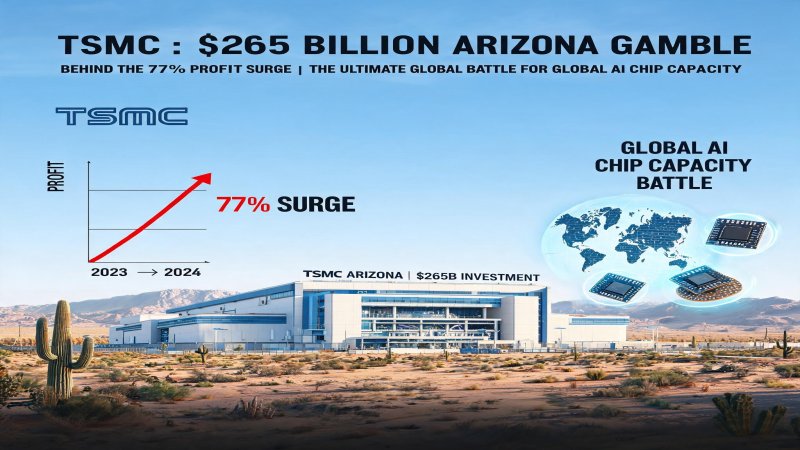
On July 17, 2026, the world's largest chip contract manufacturer, Taiwan Semiconductor Manufacturing Company (TSMC, NYSE: TSM), released its second-quarter 2026 earnings, delivering results that stunned the market. Consolidated Q2 revenue reached $40.2 billion, a 36% increase over the year-ago figure of $29.58 billion, marking the fifth consecutive quarter of record highs. Net profit climbed to $22.36 billion, a year-over-year surge of 77.4%, far exceeding the average analyst estimate of $19.5 billion. Gross margin reached 67.7%, with an operating margin of 58.2%, both sitting near historical peaks.
Simultaneously, TSMC CEO C.C. Wei announced a decision that sent shockwaves through the semiconductor industry: the company would invest an additional $100 billion in Arizona, bringing total investment commitments in the state to $265 billion. This represents the largest single-company, single-region semiconductor investment in industry history, dwarfing all previous records. Wei stated that the decision was based on a comprehensive assessment of customer demand, the geopolitical environment, and long-term strategic positioning.
The White House issued a statement approximately two hours after TSMC's announcement, confirming awareness of the investment plan and calling it "further evidence of substantive progress in rebuilding America's domestic semiconductor manufacturing capabilities." The U.S. Department of Commerce subsequently clarified that approximately 40% of the investment would qualify for subsidies under the CHIPS and Science Act, though exact amounts remained under negotiation. The Commerce Secretary described TSMC's additional investment as "a historic milestone for the U.S. semiconductor ecosystem."
Viewed through a timeline lens, TSMC's Arizona project has evolved from cautious exploration to full-scale commitment. In May 2020, TSMC first announced a $12 billion investment for a single 5nm fab in Arizona. By December 2022, the figure expanded to $40 billion with a planned second 3nm fab. In April 2024, it grew further to $165 billion, adding advanced packaging capabilities. Now, with the July 2026 commitment of $265 billion, the investment scale has multiplied 22x in just four years. This exponential escalation reflects TSMC's deep assessment of the evolving global advanced-node capacity landscape.
Notably, while TSMC was announcing these positive developments, capital markets delivered a starkly different reaction. TSMC's ADR fell for seven consecutive trading days following the earnings release, with a cumulative decline of 12.3%. The Philadelphia Semiconductor Index (SOX) dropped 15.7% over the same period, officially entering technical bear market territory (defined as a decline of more than 20% from peaks). This severe divergence between fundamentals and price action has become the most discussed market paradox.
Related intelligence was equally dense. NVIDIA denied market rumors about imminent mass production of its Vera Rubin architecture GPU, stating that next-generation products were progressing on schedule. ASML raised its second-half 2026 and full-year 2027 guidance, explicitly noting that EUV lithography equipment capacity would remain tight. Samsung Electronics announced memory chip price increases of 15-20%. AMD confirmed its next-generation EPYC Venice server processor was imminent. These information points collectively paint a complex and contradictory picture of the industry landscape.
Chapter 2: Technical Deep Dive
TSMC's technological leadership was vividly demonstrated in Q2 earnings data. Looking at process node revenue contributions, the 5nm family (including 4nm) remained the largest contributor at 33%, though this proportion declined significantly from 42% a year earlier, reflecting the rapid substitution effect of more advanced nodes. The 3nm family (including N3E, N3P) contributed 30% of revenue, surging from 18% a year ago. Most strikingly, the 2nm (N2) process contributed 3% of Q2 revenue — the industry's first commercially mass-produced 2nm node, leading Samsung and Intel by at least a quarter.
TSMC's 2nm process employs Gate-All-Around (GAA) transistor architecture, delivering approximately 15% performance improvement at the same power consumption, or 30% power reduction at the same performance level, compared to 3nm's FinFET transistors. More importantly, N2's transistor density reaches approximately 200 million transistors per square millimeter (MTr/mm2), a roughly 25% improvement over N3P's 160MTr/mm2. TSMC expects 2nm revenue share to climb to 5-7% in Q3, exceed 10% in Q4, and surpass 20% in H1 2027. This ramp speed far exceeds previous 3nm and 5nm nodes, primarily driven by strong demand from Apple's A20 chip and NVIDIA's next-generation data center GPUs.
On the more forward-looking A16 node (1.4nm, internal codename), TSMC plans to enter trial production in H2 2027. A16 will be the first to adopt Backside Power Delivery Network (BSPDN) technology combined with GAA transistor architecture, expected to deliver another generational leap in power and performance. TSMC's VP of Research stated at a technical symposium that A16 would be "the pivotal node that extends beyond traditional Moore's Law expectations."
CoWoS (Chip-on-Wafer-on-Substrate) advanced packaging technology represents another critical capacity bottleneck. During Q2, TSMC's monthly CoWoS capacity reached approximately 35,000 equivalent wafers, a 40% increase from 25,000 at end-2025. However, demand-side growth has been even more explosive. NVIDIA's Blackwell Ultra GPU, AMD's MI400 series, and various custom AI accelerator chips all heavily depend on CoWoS packaging. TSMC plans to increase monthly CoWoS capacity to 45,000 wafers by end-2026 and exceed 60,000 by mid-2027. Even so, industry analysts expect CoWoS capacity tightness to persist through 2028.
High-performance computing (HPC) at 66% of revenue became TSMC's largest business segment, further rising from 58% a year ago. This segment includes data center CPUs/GPUs, AI training and inference accelerators, and high-speed networking chips. Smartphone business accounted for approximately 25% (down from 30% a year ago), while IoT and automotive together represented about 9%. The continuing shift in revenue structure toward HPC reflects the explosive growth of AI infrastructure investment, while also implying that TSMC's revenue volatility will be increasingly tied to data center capex cycles.
The technology comparison with competitors is equally noteworthy. Intel Foundry's 18A node (1.8nm), originally planned for mass production in H2 2026, reportedly has yields hovering around 40-50%, far below the 80%+ threshold needed for commercial production. Intel recently announced a delay of 18A mass production to H1 2027. Samsung's SF2 (2nm) node also uses GAA architecture, but yields are estimated at approximately 60%, and the yield improvement rate for MBCFET transistors has been slower than expected. This means TSMC maintains at least a 12-18 month technology leadership window at the 2nm node and below, with a trend toward further widening.
ASML raised its full-year guidance after its Q2 earnings, particularly noting that low-numerical-aperture (Low-NA) EUV equipment delivery lead times remained elevated at 14-16 months. TSMC's plan to increase low-NA EUV capacity by 30% in 2027 will require significant additional equipment investment, further driving capital expenditures higher. The persistent tightness in EUV capacity, from another perspective, confirms the intensity of competition in advanced process technology.
Chapter 3: Financial Logic
TSMC's Q2 financial performance was a textbook illustration of a "super-cycle" earnings report. Revenue of $40.2 billion represented not only a 36% year-over-year increase but also a 14.8% sequential increase, marking the fifth consecutive quarter of record highs. Breaking it down, USD-denominated revenue grew 36% year-over-year, while TWD-denominated revenue grew approximately 33% (due to modest NTD appreciation against USD). Net profit of $22.36 billion translated to a net profit margin of 55.7% — virtually unheard of in the broader semiconductor industry. For comparison, Intel's net profit margin was below 10% in the same period, while Samsung's semiconductor division managed only about 20%.
The 67.7% gross margin was particularly impressive. In semiconductor manufacturing, gross margin is the core metric measuring pricing power and cost control capability. TSMC's gross margin surged more than 14 percentage points from 53.4% in Q2 2025 to 67.7%, driven by three primary factors: first, successful implementation of premium pricing strategies for advanced nodes (3nm and 2nm), where ASPs are 3-5x higher than mature nodes; second, capacity utilization maintained above 95%, effectively amortizing fixed costs; third, the continuous release of scale effects, with operating leverage significant at higher revenue bases.
However, management provided relatively cautious guidance on gross margin prospects. CFO Wendell Huang explicitly stated during the earnings call that the rapid ramp of the 2nm process in 2027 was expected to exert 3-4 percentage points of downward pressure on gross margins. This is primarily because initial yields for the 2nm node are lower than mature nodes (estimated at approximately 70-75% at initial mass production, compared to 80%+ for 3nm at its mass production debut), and depreciation costs increase significantly for the new process (a single 2nm fab requires approximately $20 billion in equipment investment). Taking these factors together, TSMC's long-term gross margin guidance is "52-58%," suggesting meaningful downside from current levels.
Regarding capital expenditure, TSMC raised its full-year 2026 capex significantly from the previous $38-42 billion to $60-64 billion, an increase of more than 50%. This capex scale exceeds Intel's and Samsung's semiconductor divisions' respective total capital expenditures. Approximately 70-80% will be allocated to advanced node (3nm, 2nm, and below) capacity construction, 10-15% to advanced packaging (primarily CoWoS expansion), with the remainder for specialty processes and R&D infrastructure. The $60-64 billion capex means TSMC's 2026 capex-to-revenue ratio will reach approximately 65-70%, a level historically seen only during the 2022 peak of approximately 55% and 2023 peak of approximately 50%.
TSMC's Q3 guidance was also robust: revenue expected at $44.6-45.8 billion (midpoint approximately $45.2 billion), gross margin expected at 65-67%, both above market expectations. Based on Q3 guidance and current order visibility, the market broadly expects TSMC's full-year 2026 revenue to exceed $160 billion, representing year-over-year growth of over 40%, further above the company's prior guidance of "above 30% growth."
However, the most perplexing aspect was the stock price performance. TSMC's ADR fell for seven consecutive trading days after the Q2 earnings release, declining from about $245 per share pre-earnings to approximately $215, a cumulative decline of 12.3%. This decline far exceeded the concurrent Nasdaq Composite (-3.2%) and S&P 500 (-1.8%). The Philadelphia Semiconductor Index dropped 15.7% over the same period, declining more than 22% from its February all-time high, officially entering technical bear market territory.
The severe divergence between stock price and fundamentals can be understood from several angles. First, the market may have fully priced in TSMC's strong results in advance (TSMC ADR had risen 25% in the three months prior to earnings), and the "buy the rumor, sell the news" trading pattern played out once again. Second, the systematic decline of the Philadelphia Semiconductor Index may have dragged down all constituent stocks indiscriminately, with panic selling in a technical bear market environment making it difficult to differentiate individual fundamentals. Third, investors may be concerned about TSMC's future gross margin trajectory (3-4 percentage points of pressure from 2nm ramp) and the cost disadvantage of overseas fabs (Arizona operations cost approximately 2-3x Taiwan operations). Fourth, macro-level uncertainties — including post-U.S. election trade policy directions and concerns about slowing global AI investment growth — are compressing the semiconductor sector's overall valuation.
Chapter 4: Strategic Depth
To truly understand the strategic intent behind TSMC's $265 billion Arizona investment, it must be examined within the broader landscape of global semiconductor competition. The following competitive comparison matrix clearly illustrates the core differences among the three major foundries:
| Dimension | TSMC | Intel Foundry | Samsung Foundry |
|---|---|---|---|
| Most Advanced Mass Production Node | N2 (2nm), 3% revenue in Q2 2026 | Intel 4 (7nm), 18A (1.8nm) delayed to 2027H1 | SF2 (2nm), yield approx. 60% |
| Next-Generation Node | A16 (1.4nm), trial production 2027H2 | Intel 14A (1.4nm), planned 2028 | SF1.4 (1.4nm), planned 2028 |
| 2026 Estimated Revenue | >$160 billion | ~$20 billion (foundry segment) | ~$18-20 billion (foundry segment) |
| Gross Margin | 67.7% (Q2), long-term guide 52-58% | Loss-making (foundry division) | ~20-25% (foundry segment) |
| Capacity Scale (monthly equiv. 12-inch wafers) | >800K | ~300K | ~400K |
| Arizona Investment | $265 billion | Ohio >$40 billion (incl. IDM 2.0) | Taylor fab >$40 billion |
| Key Customers | Apple, NVIDIA, AMD, Qualcomm, Broadcom | Intel internal use + few external | Qualcomm (partial), Google (partial) |
| Advanced Packaging | CoWoS, InFO, SoIC | Foveros, EMIB | I-Cube, X-Cube |
| EUV Equipment Fleet | >100 units (incl. High-NA) | ~40 units | ~30 units |
| 2nm Capacity (2027 estimate) | >150K equiv. wafers/month | Uncertain | ~20-30K wafers/month |
The geopolitical drivers behind the $265 billion Arizona investment cannot be overlooked. The U.S. CHIPS and Science Act provides $52.7 billion in direct subsidies and tax incentives, serving as a significant external catalyst for TSMC's investment decision. More importantly, TSMC's major customers — Apple, NVIDIA, AMD, Qualcomm, and others — are predominantly American companies facing increasing pressure for localized supply chains. Demand from U.S. Department of Defense and DARPA for "secure supply chains" is also pushing advanced-node production capacity toward the U.S. mainland.
TSMC's customer diversification strategy is also noteworthy. Although HPC dominates at 66% of revenue, TSMC is actively expanding into automotive chips (partnering with Bosch, Toyota, etc.), IoT (deeply embedded in the ARM ecosystem), and RF/analog specialty processes. However, an unavoidable reality is that TSMC's revenue concentration is increasing — Apple and NVIDIA alone account for over 40% of revenue. This high concentration is both a source of TSMC's pricing power and a potential risk point.
From a vertical integration perspective, TSMC is evolving from a pure "manufacturing service provider" to a "technology ecosystem platform." By integrating advanced processes (N2/A16), advanced packaging (CoWoS/SoIC), design IP (OIP platform), and EDA toolchain partnerships, TSMC provides customers with an end-to-end solution from design to mass production. This vertical integration capability further raises the barrier to entry for new players and competitors.
In terms of capacity layout, TSMC's globalization strategy has evolved from "Taiwan-centric manufacturing" to "Taiwan core + multi-site complement." Beyond the $265 billion Arizona investment, TSMC's Kumamoto fab (JASM) in Japan has already entered mass production, its Dresden fab (ESMC) in Germany is under construction with planned 2027 production. This multi-site layout is both a defensive strategy against geopolitical risk and an offensive strategy to get closer to major customers. However, it should be noted that overseas fabs always lag Taiwan's leading-edge nodes by at least one generation — Arizona currently mass-produces 5nm, Kumamoto produces 4nm/3nm, while Taiwan is already mass-producing 2nm. This deliberate "technology generation gap" is a key design element protecting TSMC's core competitiveness.
Chapter 5: Challenges and Concerns
Despite TSMC's impeccable fundamental performance, risk factors are accumulating across multiple dimensions that warrant close attention.
First, the signal of seven consecutive days of stock decline and the Philadelphia Semiconductor Index entering technical bear market territory should not be ignored. Over the past two weeks, the Philadelphia Semiconductor Index has retreated more than 22% from its June high, exceeding the 20% technical bear market definition. This decline is not specific to TSMC but represents a systematic correction across the entire semiconductor sector. NVIDIA, AMD, Broadcom, Qualcomm, and other AI-related chip stocks all experienced double-digit declines. Driving factors include: concerns about slowing AI infrastructure investment growth (capex growth rates at hyperscale cloud companies including Microsoft, Google, and Meta showed deceleration signs in H1 2026); global interest rate uncertainty raising discount rates for tech stocks; and institutional investors taking profits in the semiconductor sector.
For TSMC specifically, the divergence between stock price and fundamentals presents both risk and opportunity. If the AI investment cycle has indeed peaked and begun rolling over, the current valuation (approximately 22x forward P/E, a premium to the 5-year average of 18x) may still have downside room. Conversely, if the AI investment cycle continues robust, the current pullback would offer an attractive entry point. The key lies in assessing the ratio of "real demand" versus "inventory hoarding demand" in AI infrastructure investment.
Second, while the 2nm process ramp is faster than previous nodes, its suppressive effect on gross margins should not be overlooked. TSMC management explicitly expects the 2nm ramp to exert 3-4 percentage points of downward pressure on gross margins. From historical experience, initial yields for new process mass production are typically 10-20 percentage points below mature nodes, and each percentage point improvement in yield translates to approximately 0.3-0.5 percentage points of gross margin improvement. Additionally, 2nm fab depreciation costs are significantly higher than 3nm and 5nm — a single 2nm fab requires approximately $20 billion in equipment investment, translating to monthly depreciation of approximately $330 million over a 5-year depreciation schedule. Until 2nm's revenue contribution exceeds 20%, depreciation pressure will persist.
Third, the cost disadvantage of overseas fabs is a persistent structural issue. TSMC's Arizona fab operating costs (including labor, land, energy, logistics, etc.) are approximately 2-3x those of Taiwan facilities. Although U.S. CHIPS Act subsidies can partially offset this cost disadvantage, subsidies are one-time while the cost disadvantage is ongoing. This means chips produced in Arizona will carry significantly higher costs than equivalent chips produced in Taiwan, and how to absorb this cost differential in pricing strategy is a challenge TSMC must face long-term.
Fourth, the impact of Chinese AI models is an underestimated risk factor. Over the past year, Chinese technology companies (including DeepSeek, Baidu, Alibaba, ByteDance, and others) have made significant progress in AI large language models, with some models approaching GPT-4-level capabilities. These advances have been achieved primarily on domestic AI chips (such as Huawei's Ascend series) or hybrid architectures, reducing dependence on NVIDIA's high-end GPUs. If the trend of Chinese AI chip self-sufficiency continues to accelerate, it would indirectly impact NVIDIA's and other TSMC core customers' shipment volume expectations, thereby affecting TSMC's long-term growth narrative.
Fifth, concentration risk deserves vigilance. TSMC's revenue is highly concentrated among a few large customers and a few advanced process nodes. Apple alone contributes approximately 25% of revenue, NVIDIA about 15-18%, with the combined total exceeding 40%. By process node, 3nm and 5nm together contribute 63% of revenue. This high concentration means that if any major customer significantly reduces orders (e.g., Apple shifting to in-house chip manufacturing or changing foundry partners, though extremely unlikely), TSMC would face significant revenue volatility.
Chapter 6: Conclusion
TSMC's Q2 2026 performance and the $265 billion Arizona investment plan together paint a picture of "technological leadership, strategic ambition, and robust fundamentals." However, consecutive stock price declines and the Philadelphia Semiconductor Index's bear market signal remind us that the relationship between market sentiment and fundamentals is complex and nuanced.
For chip buyers, TSMC's capacity planning and process roadmap directly determine supply chain security. Key action items include: first, immediately assess 2027 CoWoS advanced packaging capacity needs and initiate reservations, as the capacity window is extremely short; second, establish closer technical cooperation with TSMC (through the OIP platform) to secure priority allocation at the 2nm and A16 nodes; third, consider a "Taiwan + overseas" dual-source strategy to diversify geopolitical risk; fourth, begin adapting AI accelerator chip designs for CoWoS-L and SoIC advanced packaging solutions early, as packaging capacity is the key bottleneck determining delivery timelines.
For investors, TSMC's fundamentals remain exceptionally strong, but valuations have risen above historical averages. In the Philadelphia Semiconductor Index's technical bear market environment, a phased entry strategy is recommended, with close attention to the following catalysts: the actual 2nm revenue ramp speed in Q3 earnings (expected mid-August release); specific funding arrangements and timeline for the Arizona investment; progress in CHIPS Act subsidy negotiations; and the next-generation product release cadence of core customers like NVIDIA and Apple. Long-term investors should focus on TSMC's R&D progress at the A16 (1.4nm) node and its ability to maintain the technology leadership window.
For competitors (Intel Foundry and Samsung Foundry), the fact that TSMC's 2nm already contributed revenue in Q2 means the catch-up window is narrowing, not widening. Intel needs to achieve breakthrough progress on 18A node yield ramp, otherwise its foundry business faces increasing customer attrition risk. Samsung needs to make substantial improvements in SF2 yield and capacity while leveraging its memory chip strengths to build an integrated "logic + memory" one-stop solution. Overall, TSMC's dominant position in the global advanced-node foundry market appears unassailable in the foreseeable future, though geopolitical factors and cost pressures from capacity expansion are challenges shared by all participants.
TSMC's $265 billion Arizona gamble is not merely a corporate strategic decision — it is a landmark event reshaping the global semiconductor supply chain landscape in the AI era. It simultaneously answers two questions: How will the AI chip capacity bottleneck be broken? And, amid global geopolitical competition, where will the "redistribution" of advanced manufacturing capabilities lead? Regardless of the answers, TSMC has placed its bet with real money.
Why it Matters
TSMC's moves are not merely corporate financial events — they are pivotal signals reshaping the global semiconductor landscape. The $265 billion Arizona investment means U.S. domestic advanced-node capacity will jump from near-zero to a significant share of global output, profoundly altering the geopolitical map of the chip supply chain. For AI chip buyers, TSMC's capacity planning and technology roadmap directly determine the delivery capabilities and cost structures of next-generation products from NVIDIA, AMD, Apple, and other key customers.
DECISION
Chip Buyers (Cloud/AI startups): Immediately lock in 2027 CoWoS advanced packaging capacity — the battle for 3nm and 2nm allocation is already fierce, and delayed orders mean a 6-12 month delivery gap. Investors: The current 7-day consecutive stock decline may offer a mid-term buying window, as fundamentals (67.7% gross margin, 77% profit growth) severely diverge from price action, though watch for systemic risks amid the Philadelphia Semiconductor Index bear market. Competitors (Intel/Samsung): TSMC's 2nm contributing revenue in Q2 means the technology leadership window is widening — chasers must re-evaluate their process roadmaps and capex strategies. Equipment Suppliers (ASML etc.): TSMC raising capex to $60-64 billion and planning 30% low-NA EUV capacity growth in 2027 signals confirmed EUV lithography order increases.
PREDICT
Q3 2026: TSMC revenue will reach the $44.6-45.8 billion range, gross margin staying elevated at 65-67%, 2nm share climbing to 5-7%, with Apple A20 and NVIDIA Blackwell Ultra entering mass production. Q4 2026: 2nm share may exceed 10%, CoWoS monthly capacity surpassing 40,000 wafers, and AMD EPYC Venice processors beginning shipments. H1 2027: Arizona's first 2nm fab begins risk production, low-NA EUV capacity increases 30%, while Intel 18A remains in yield ramp. H2 2027: Samsung 2nm (SF2) enters mass production, TSMC A16 (1.4nm) enters trial production, and global advanced-node capacity competition intensifies dramatically.
Get 3-5 key AI infrastructure signals weekly →
💬 Comments (0)