
<h2>I. Event Recap: Record Earnings Meet a $265 Billion Geopolitical Bet</h2>
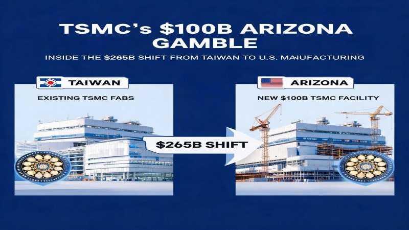
<p>On July 16, 2026, TSMC Chairman and CEO C.C. Wei dropped two bombshells during the company’s Q2 earnings call. First, TSMC reported a record-breaking net profit of NT$706.56 billion (approximately $22.08 billion), surging 77.4% year-over-year. Second, and arguably more consequential, the company announced an additional $100 billion commitment to its Arizona manufacturing complex, raising its total U.S. investment pledge from $165 billion to $265 billion—an amount Wei characterized as the largest foreign direct investment in American history.</p>
<p>The financial metrics for Q2 were nothing short of spectacular. Revenue reached $40.2 billion, hitting the very top of the guided range of $39.0–$40.2 billion. In local currency, that translates to roughly NT$1.27 trillion, representing 36% year-over-year growth and 12% sequential growth. Gross margin held firm at an extraordinary 67.7%, with operating margin at 60.3% and net profit margin at 55.6%. Diluted earnings per share came in at NT$27.25, equivalent to approximately $4.31 per ADR. For the first half of 2026, cumulative revenue hit NT$2.40 trillion (up 35.6% YoY), while net profit soared 68.3% to NT$1.28 trillion.</p>
<p>Management’s forward guidance was equally aggressive. Q3 revenue is projected at approximately $44.6 billion, which would set yet another quarterly record. More significantly, TSMC raised its full-year 2026 capital expenditure guidance from $52.0–$56.0 billion to $60.0–$64.0 billion, an upward revision of 15–23%. Between 70% and 80% of this capex will be directed toward advanced process technologies, primarily 3nm and 2nm capacity expansion.</p>
<p>Yet the market’s reaction was paradoxically negative. TSMC’s ADR fell 3.5–4% following the announcement. The disconnect between stellar fundamentals and stock price performance reflects a deeper investor anxiety: while the $265 billion Arizona commitment cements TSMC’s alignment with American tech giants like Apple and NVIDIA, it also introduces material risks around margin compression, geopolitical uncertainty, and the well-documented reality that building fabs in the U.S. costs 30–50% more than in Taiwan.</p>
<h2>II. Technical Deep Dive: How 2nm Redefines Semiconductor Physics</h2>
<p>The additional $100 billion is earmarked for fabs producing "2nm and below" logic chips, plus advanced packaging facilities. To grasp the magnitude of this technological leap, one must understand the architectural revolution TSMC is orchestrating from N3E to N2.</p>
<p><strong>From FinFET to GAAFET: The Transistor Architecture Revolution</strong></p>
<p>TSMC’s N2 process is the world’s first high-volume manufacturing node to deploy Gate-All-Around FET (GAAFET, also known as Nanosheet) transistors. Unlike the FinFET architecture used in N3E, where the gate wraps around three sides of a vertical fin, GAAFET completely surrounds the channel with gate material on all four sides. This delivers superior electrostatic control, dramatically reducing leakage current and short-channel effects that have plagued FinFET designs below 3nm.</p>
<p>According to TSMC’s official disclosures, compared to N3E, N2 delivers 10–15% higher performance at iso-power and iso-complexity; 25–30% lower power consumption at iso-frequency and iso-transistor-count; and a 10–20% improvement in logic density. The aggregate performance gain approaches 30% for typical implementations. For Apple’s A20 Pro, NVIDIA’s Rubin-architecture GPUs, and AMD’s Zen 6 processors, this translates to meaningful headroom—either higher performance within the same thermal envelope, or substantially improved battery life at equivalent compute levels.</p>
<p><strong>Backside Power Delivery: Unclogging the Interconnect Bottleneck</strong></p>
<p>N2 also introduces Backside Power Delivery Network (BSPDN), a structural innovation that moves power routing to the backside of the wafer. Traditionally, both signal interconnects and power/ground networks compete for precious frontside routing resources. As transistor density increases, power rails consume an ever-growing share of available metal layers, choking signal paths and increasing IR drop. By relocating power delivery to the wafer backside, N2 frees the entire frontside for signal routing, improving density by an additional 10–15% and enabling high-performance cores to operate stably at lower voltages.</p>
<p><strong>Arizona’s Technology Roadmap</strong></p>
<p>TSMC Arizona (Fab 21) is rapidly escalating its technology portfolio. Fab 1 is in pre-production qualification; Fab 2 completed structural construction in 2025 and targets N3 volume production in the second half of 2027. Fab 3 broke ground in April 2025 with a goal of production by the end of the decade. The newly announced $100 billion injection will fund at least four additional 2nm-class fabs, bringing the Arizona campus to a total of 10 wafer fabs, 2 advanced packaging facilities, and 1 R&D center.</p>
<p><strong>Advanced Packaging: The Real AI Bottleneck</strong></p>
<p>Perhaps the most strategically consequential element of the expanded investment is the addition of two advanced packaging facilities. The binding constraint on AI accelerator supply today is not wafer fabrication—it is CoWoS (Chip on Wafer on Substrate) packaging capacity. CoWoS is the 2.5D integration technology that bonds AI compute dies to High Bandwidth Memory (HBM) via a silicon interposer, enabling products like NVIDIA’s H100, H200, and B200 to function as shippable systems. TSMC’s CoWoS lines have already achieved mass production of 5.5x reticle-size products with yields exceeding 98%. The roadmap calls for 14x reticle-size products supporting 20 HBMs by 2028, and even larger configurations integrating 24 HBMs by 2029.</p>
<p>The Arizona packaging complex will also introduce SoIC (System-on-Integrated-Chips) and CoPoS (Chip-on-Panel-on-Substrate). SoIC represents TSMC’s most advanced 3D packaging approach, using direct bonding to achieve vertical chip stacking with interconnect densities far beyond traditional microbump technologies. It is the critical enabler for next-generation AI chips pursuing compute-in-memory architectures.</p>
<h2>III. Financial Logic: Decoding the ROI of a $265 Billion Bet</h2>
<p>To put $265 billion in perspective: it exceeds the annual GDP of countries like Finland and Portugal, and equals roughly 55% of Vietnam’s 2025 GDP. Why would TSMC stake such an astronomical sum?</p>
<p><strong>Q2 Earnings Decomposition: The AI Profit Engine</strong></p>
<p>Within TSMC’s $40.2 billion Q2 revenue, the High-Performance Computing (HPC) platform has overtaken smartphones as the largest revenue contributor, with AI-related chips serving as the primary growth vector. NVIDIA’s B200/B300 series, AMD’s MI350, Google’s TPU v6, and Amazon’s Trainium3 are all ramping on TSMC’s 3nm and 4nm nodes. Processes at 7nm and below accounted for approximately 70% of total wafer revenue—a structural trend that continuously strengthens TSMC’s pricing power. N3E wafer prices have already breached $20,000 per wafer, and upcoming N2 wafers are expected to command $25,000–$30,000.</p>
<p><strong>The Strategic Signal Behind Capex Guidance</strong></p>
<p>Raising 2026 capex from $52–56 billion to $60–64 billion signals management’s extraordinary confidence in the durability of AI chip demand. With a typical semiconductor fab payback period of 3–5 years, this spending wave will convert to revenue between 2029 and 2031. Assuming an N2 wafer price of $25,000 and a per-fab capacity of 30,000 wafers per month (WPM), a single 2nm fab at full utilization generates $9–11 billion in annual revenue. Four such fabs would contribute $36–44 billion annually—representing roughly 25–30% of TSMC’s projected 2026 total revenue.</p>
<p><strong>Quantifying Gross Margin Pressure</strong></p>
<p>Despite the revenue upside, 2nm ramp-up will exert meaningful pressure on gross margins. New-node initial yields typically hover in the 60–70% range, far below the 90%+ achieved at mature nodes, inflating effective wafer costs dramatically. Meanwhile, the 30–50% U.S. construction cost premium means Arizona fabs will carry significantly higher depreciation charges than their Taiwan counterparts. TSMC maintains a long-term gross margin target above 53%, but during the 2027–2028 N2 ramp, margins could compress to the 60–62% range from the current 67.7%. This margin trajectory—not the headline earnings beat—explains why the stock sold off on what appeared to be unambiguously positive news.</p>
<p><strong>The ROI Equation</strong></p>
<p>The $265 billion investment’s return hinges on three variables: Arizona fab utilization rates, N2/N2P wafer pricing power, and the margin premium from advanced packaging (CoWoS/SoIC). If AI chip demand sustains a 25%+ CAGR through 2030 and TSMC preserves its yield leadership over Samsung and Intel (currently N2 yields of ~78–90% versus Samsung SF2 at 50–60% and Intel 18A at ~85%), the project could achieve positive net present value (NPV) between 2032 and 2035.</p>
<h2>IV. Strategic Landscape: How the Foundry Triopoly Is Reshaping</h2>
<p>TSMC’s $265 billion Arizona commitment is rewriting the competitive map of global semiconductor manufacturing. The following matrix compares TSMC, Samsung Foundry, and Intel Foundry across four critical dimensions:</p>
| Dimension | TSMC | Samsung Foundry | Intel Foundry |
|---|---|---|---|
| Process Node & Yield (2nm-class) | N2 in mass production; 78–90% yield; GAAFET + BSPDN | SF2 (2nm) at 50–60% yield; GAAFET; targeting 21,000 WPM by end-2026 | 18A at ~85% yield; RibbonFET (GAA); ~30,000 WPM capacity |
| Global Capacity Footprint | Taiwan dominant (11 fabs at ≤2nm), Arizona (10 fabs), Kumamoto Japan, Dresden Germany | Korea Pyeongtaek P5/P6 core; Taylor Texas fab starting H2 2026 | Oregon, Arizona, New Mexico USA; European expansion planned; 18A concentrated in U.S. |
| Customer Mix | Apple, NVIDIA, AMD, Qualcomm, MediaTek, Broadcom, Amazon, Google | Samsung internal, partial Qualcomm, Tesla (AI6 chip), select Chinese customers | Intel internal products dominant; external: Amazon, Microsoft (rumored); external revenue share still low |
| 2026 Capital Expenditure | $60.0–$64.0 billion (revised upward); 70–80% to advanced nodes | ~$30.0–$35.0 billion (foundry share ~30% of group semiconductor investment) | ~$20.0–$25.0 billion (contracted since Intel Foundry spin-out) |
| Advanced Packaging | CoWoS (2.5D), SoIC (3D), InFO; CoWoS yield >98% | I-Cube (2.5D), X-Cube (3D); capacity and yield lag TSMC | EMIB (2.5D), Foveros (3D); primarily serving Intel internal products |
| Market Share (Q2 2025) | 70.2% (record high) | 7.3% | ~2–3% (pure external foundry revenue) |
<p>The competitive matrix reveals a stark reality: TSMC holds dominant positions across process leadership, customer ecosystem, manufacturing scale, and advanced packaging depth. Samsung Foundry, despite being an early mover in GAAFET deployment, faces a crippling yield gap—SF2 at 50–60% is nowhere near the stability threshold demanded by tier-one customers like Apple and NVIDIA. Samsung’s pricing strategy undercuts TSMC by 15–20%, but in the AI chip market, customers prioritize yield consistency and delivery certainty over unit cost.</p>
<p>Intel Foundry has made remarkable yield progress on 18A, narrowing the technical gap with TSMC. Yet its fundamental dilemma—the conflict between internal and external customers—remains unresolved. When Intel’s own products (such as Nova Lake compute tiles) consume priority 18A capacity, external customers struggle to secure firm allocation guarantees. Moreover, Intel Foundry’s advanced packaging capabilities remain largely captive to internal products, lacking the open-market CoWoS-scale delivery that hyperscalers require.</p>
<p>GlobalFoundries exited the 7nm-and-below race years ago, focusing on 12nm–28nm mature nodes and specialty processes (RF-SOI, SiGe). In the AI compute battlefield that matters most, TSMC effectively operates in a "one superpower, no strong challengers" oligopoly.</p>
<h2>V. Challenges and Concerns: The Risk Map Behind $265 Billion</h2>
<p>Despite its unassailable technological and market position, TSMC’s $265 billion U.S. investment exposes deep strategic anxieties that the company can no longer ignore.</p>
<p><strong>Geopolitical Risk: A Forced Migration from "Made in Taiwan" to "Made in America"</strong></p>
<p>The primary driver behind TSMC’s Arizona expansion is not commercial optimization—it is geopolitical insurance. The U.S. CHIPS and Science Act offers $52.7 billion in subsidies, but with strings attached requiring advanced manufacturing on American soil. As U.S.-China tech decoupling accelerates, American customers—especially in defense and AI infrastructure—are demanding "non-China" supply chains with increasing urgency. By building 10 fabs in Arizona, TSMC is essentially buying insurance against the worst-case scenario of cross-strait conflict. However, if geopolitical tensions ease or U.S. policy shifts after the 2028 election cycle, the commercial return on this investment becomes far more uncertain.</p>
<p><strong>Talent Shortage: The 100,000-Engineer Gap</strong></p>
<p>Fab construction and operation depend on deeply specialized engineering talent. TSMC’s Arizona Fab 1 has already experienced significant cultural friction and talent attrition—Taiwanese technical leaders and American local workers clash over management styles and work pacing. The broader U.S. semiconductor industry faces a shortage exceeding 100,000 engineers. While Arizona State University provides a solid pipeline, training enough process engineers, equipment specialists, and yield analysts for 10 wafer fabs and 2 packaging plants will require 5–10 years. Talent bottlenecks could push Arizona production timelines behind schedule.</p>
<p><strong>Cost Structure: The 30–50% U.S. Premium</strong></p>
<p>TSMC management has repeatedly acknowledged on earnings calls that U.S. fab construction costs 30–50% more than in Taiwan. This premium stems from multiple sources: construction labor costs (unionized U.S. crews work at materially lower efficiency than Taiwanese counterparts), equipment import tariffs and logistics, and stricter U.S. environmental and safety compliance. Water is another constraint—Arizona is desert, yet wafer manufacturing is extraordinarily water-intensive (~2–3 tons of ultrapure water per wafer). TSMC has pledged recycling technologies, but long-term water security remains a latent risk.</p>
<p><strong>Gross Margin Compression: The Slide from 67.7% to 60%</strong></p>
<p>As detailed earlier, the dual squeeze of 2nm yield ramp and high-cost U.S. capacity could materially compress gross margins over the next 2–3 years. A decline from 67.7% to 60–62% would significantly slow net profit growth even if revenue sustains 15–20% annual expansion. Investors accustomed to TSMC’s "revenue and profit double-growth" paradigm will need time to adjust. This valuation recalibration—not operational deterioration—drove the 3.5–4% ADR decline.</p>
<p><strong>Customer Concentration: The NVIDIA-Apple Dependency</strong></p>
<p>TSMC’s top five customers (Apple, NVIDIA, AMD, Qualcomm, MediaTek) contribute over 60% of revenue, with NVIDIA and Apple likely approaching 40% combined. If AI chip demand experiences a cyclical correction in 2027–2028, or if Apple reduces A-series orders as it brings more silicon in-house, TSMC’s utilization rates would face severe pressure. The absorption of $265 billion in new capacity depends heavily on the persistence of AI-driven demand.</p>
<h2>VI. Conclusion: Finding an Anchor Between Certainty and Uncertainty</h2>
<p>TSMC’s $265 billion Arizona commitment represents the largest single geographic capacity migration in semiconductor history. It is more than a corporate investment decision—it is the defining event of a global supply chain pivoting from "efficiency-first" to "resilience-first." For decision-makers across different roles, we offer the following actionable recommendations:</p>
<p><strong>For Fabless Chip Companies and Procurement Leaders:</strong></p>
<p>1. <strong>Secure N2 capacity windows immediately</strong>: TSMC’s N2 capacity is expected to ramp beyond 50,000 WPM by 2027, but first-year output is already booked by Apple, NVIDIA, and other top-tier customers. If you have 2nm tape-out requirements, initiate engagement with TSMC account managers now to secure allocation for Q2–Q3 2028. For smaller chip companies, leverage MPW (Multi-Project Wafer) services to validate N2 designs early.</p>
<p>2. <strong>Diversify advanced packaging supplier risk</strong>: CoWoS is the hard bottleneck for AI chips, and TSMC’s dominance will persist through at least 2028. Evaluate InFO and SoIC alternatives during the design phase, and establish relationships with secondary packaging providers like Amkor and ASE to prepare for capacity relief post-2029.</p>
<p>3. <strong>Reassess Samsung as a viable backup</strong>: Samsung SF2 offers 15–20% pricing discounts versus TSMC N2 and is aggressively pursuing Qualcomm, Tesla, and others. For non-tier-one chip companies with more relaxed yield requirements (consumer IoT, automotive MCUs), conduct small-volume qualification runs with Samsung as a second-source strategy.</p>
<p><strong>For Institutional Investors and Equity Holders:</strong></p>
<p>1. <strong>Short-term (6–12 months): Exercise caution</strong>: Despite the Q2 beat, the capex increase and margin overhang will constrain valuation expansion. Consider accumulating TSMC ADRs on pullbacks to the $150–160 range (implying 18–20x 2026E P/E).</p>
<p>2. <strong>Medium-term (2–3 years): Monitor N2 yield trajectory</strong>: If N2 yields stabilize above 85% by late 2027 and Arizona Fab 3 comes online as scheduled, TSMC re-enters a "dual-revenue-profit-growth" trajectory with a price target of $220–240.</p>
<p>3. <strong>Long-term (5+ years): Bet on AI compute infrastructure</strong>: The $265 billion investment is fundamentally a 15-year wager on sustained AI compute demand. If you believe Artificial General Intelligence (AGI) will arrive before 2030 and trigger exponential compute requirements, TSMC remains one of the most compelling long-duration semiconductor holdings globally.</p>
<p><strong>For Policy Researchers and Industry Analysts:</strong></p>
<p>The key variable shaping TSMC’s U.S. investment is the post-2028 American administration’s China policy. If the next government intensifies chip export controls, Arizona becomes the "heart" of America’s AI chip supply chain, with strategic value dwarfing financial returns. Conversely, if U.S.-China tensions de-escalate, American customers may re-evaluate the cost-effectiveness of a dual "Taiwan + U.S." sourcing model, exposing TSMC to periods of regional overcapacity.</p>
<p>Regardless of geopolitical outcomes, one fact is immutable: in the 2nm-and-below frontier, TSMC’s technical lead (yield advantages of 20–30 percentage points over Samsung), customer ecosystem breadth (8 of the world’s top 10 chip designers), and manufacturing scale (10 Arizona fabs plus 11 Taiwan fabs at ≤2nm) will construct an almost unbreachable moat for the next 5–8 years. The $265 billion is not a gamble—it is a strategic depth play, exchanging capital for time and space. For the entire technology ecosystem that depends on leading-edge silicon, every expansion step TSMC takes redraws the boundaries of AI-era compute.</p>
Why it Matters
TSMC's additional $100 billion commitment, raising total Arizona investment to $265 billion, represents not only the largest single geographic capacity migration in semiconductor history, but also signals a paradigm shift from 'efficiency-first' to 'resilience-first' global chip supply chains. With AI compute demand growing at 25%+ annually, this move effectively locks in U.S. AI infrastructure wafer supply for the next decade. For customers like Apple, NVIDIA, and AMD, the Arizona complex becomes geopolitical insurance. It also widens TSMC's technological lead over Samsung Foundry (SF2 yield 50–60%) and Intel Foundry (18A yield ~85%), cementing its dominant >70% foundry market share.
DECISION
【For Fabless Companies & Procurement Leaders】
- Secure N2 capacity immediately: First-year N2 output is booked by Apple/NVIDIA; initiate TSMC engagement now for Q2–Q3 2028 allocation. Smaller companies should use MPW services for early N2 validation.
- Diversify packaging risk: CoWoS bottleneck persists through 2028; evaluate InFO/SoIC alternatives and establish secondary relationships with Amkor and ASE.
- Assess Samsung as backup: SF2 offers 15–20% pricing discounts; suitable for consumer/ automotive chips with relaxed yield requirements.
【For Institutional Investors】
- Short-term (6–12 months): Exercise caution; accumulate on pullbacks to $150–160 (18–20x 2026E P/E).
- Medium-term (2–3 years): Monitor N2 yield ramp; if yields stabilize above 85% by late 2027, price target $220–240.
- Long-term (5+ years): A 15-year wager on sustained AI compute demand; among the most compelling long-duration semiconductor holdings globally.
PREDICT
- 【Q4 2026】TSMC Arizona Fab 1 (N4 process) enters volume production, with initial output likely targeting Apple Watch or entry-level iPhone chips.
- 【H2 2027】N2 achieves mass production in Taiwan exceeding 50,000 WPM; Arizona Fab 2 (N3) begins volume production. U.S.-produced wafers will cost 30–50% more than Taiwan equivalents, compressing blended gross margins to 60–62%.
- 【2028】Arizona advanced packaging plant (AP1) breaks ground, introducing SoIC and CoPoS technologies. CoWoS bottleneck partially eases, but AI chip demand growth maintains tight supply-demand balance.
- 【Before 2030】If AI compute demand sustains 25%+ CAGR, Arizona could generate $36–44 billion annual revenue from four 2nm fabs at full utilization, contributing 25–30% of TSMC total revenue.
Get 3-5 key AI infrastructure signals weekly →
💬 Comments (0)