
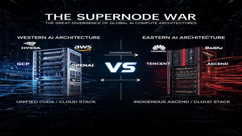
The Supernode War: The Great Divergence of Global AI Compute Architectures
Summary
In 2026, AI supernodes have become the central battlefield of compute competition. NVIDIA's NVLink 6.0 achieves 3.6 TB/s per-GPU bandwidth but remains constrained to a 72-GPU full-switch domain; Google's TPU v7 sets a scale record with a 9,216-chip Superpod; Huawei's Ascend Atlas 950 enters the top tier with 8,192 NPUs and its Lingqu all-optical switching fabric; AMD's Helios marks the first rack-level system directly benchmarking against NVL72 with 72 accelerators. These four architectures make fundamentally different engineering trade-offs in interconnect topology, bandwidth density, scalability limits, and software ecosystems, driving AI infrastructure from "single-GPU dominance" toward a "multi-architecture coexistence" paradigm.
Event Overview
The first half of 2026 saw a wave of supernode announcements. At CES in January, NVIDIA unveiled Vera Rubin NVL72, doubling per-GPU interconnect bandwidth to 3.6 TB/s with rack-level aggregate bandwidth of 260 TB/s ✅ Verified. In April, Google launched TPU v7 Ironwood Superpod featuring 9,216 liquid-cooled chips, 42.5 EFLOPS of FP8 compute, and 1.77 PB of memory ⚠️ Vendor claim. At WAIC 2026 in June, Huawei showcased the Atlas 950 SuperPoD in physical form for the first time, supporting up to 8,192 Ascend NPUs with Lingqu 2.0 delivering 16.3 PB/s of all-optical interconnect bandwidth ⚠️ Vendor claim. That same month at Computex, AMD debuted its Helios rack-scale system integrating 72 MI455X accelerators, 31 TB of HBM4 memory, and 2.9 EFLOPS of FP4 throughput ⚠️ Vendor claim.
These four products embody four entirely distinct supernode design philosophies: full-switch GPU, 3D Torus mega-Pod, hierarchical Mesh with optical switching, and ring-topology rack-scale.
Technical Deep Dive: Six-Dimensional Comparison
I. Interconnect Topology — The Architectural DNA
The core challenge of a supernode is connecting dozens to thousands of chips into a logically unified compute system. The interconnect topology determines all downstream performance characteristics.
NVIDIA chose full-mesh via NVSwitch: 72 GPUs each connect through 18 NVLink lanes to 9 NVSwitch ASICs, enabling single-hop communication between any pair with 130 TB/s aggregate bandwidth (GB300 NVL72) and latency of approximately 0.5–1 microsecond ✅ Verified. This delivers the highest bandwidth and lowest latency, but switch port count scales quadratically with GPU count—72 GPUs already approaches the physical limit of NVSwitch port density.
Google chose 3D Torus: 9,216 TPUs arranged in a three-dimensional grid, each chip directly connected to 6 neighbors, with ICI bandwidth of 9.6 Tb/s (~1.2 TB/s) ⚠️ Vendor claim. No centralized switch chips are needed, keeping costs manageable, but remote communication requires multiple hops with effective bandwidth degrading over distance. Google mitigates this through OCS (Optical Circuit Switch) reconfiguration at millisecond timescales.
Huawei chose a UB-Mesh hybrid topology: 64 NPUs within each cabinet connect via 2D-Mesh over electrical links, while cabinets link through Lingqu OCS all-optical switches, creating a "short-range electrical + long-range optical" layered architecture ⚠️ Vendor claim. The core idea is matching different parallelism communication patterns (tensor, data, expert parallelism) to the optimal physical topology layer—Huawei claims this reduces networking costs by approximately 5x.
AMD chose a Ring topology: 8-GPU nodes connect in a P2P ring, scaling to 72 GPUs in the Helios rack ⚠️ Vendor claim. Simple to implement without switch chips, but All-to-All communication efficiency is inversely proportional to GPU count (Ring All-Reduce efficiency equals 2(N-1)/N), creating inherent disadvantages in large-scale global communication scenarios.
II. Bandwidth Density — How Much Data Each Chip Can Consume
| Solution | Per-Chip Interconnect BW | Topology | Effective BW Characteristic |
|---|---|---|---|
| NVIDIA NVLink 6.0 | 3.6 TB/s | Full-switch | Full BW between any pair, no contention |
| NVIDIA NVLink 5.0 | 1.8 TB/s | Full-switch | Same (current volume production) |
| Groq 3 LPU C2C | 2.5 TB/s | Dragonfly | Weights resident on-chip, only activations flow |
| Google TPU v7 ICI | ~1.2 TB/s | 3D Torus | Full BW to neighbors, degrades with distance |
| AMD MI350X IF | ~1.2 TB/s | Ring | Global comm efficiency declines with scale |
| Huawei Ascend 950 | ~2.0 TB/s | UB-Mesh | Layered BW: high intra-cabinet, optical inter-cabinet |
III. Scalability Limits — Maximum Chips per Domain
| Solution | Max Single-Domain Scale | Scale-Out Method |
|---|---|---|
| Google TPU v7 | 9,216 chips/Superpod | Jupiter datacenter network, 100K+ chips |
| Huawei Atlas 950 | 8,192 NPUs | 64 supernodes further interconnected |
| NVIDIA NVLink domain | 72 GPUs (Rubin plans 144) | InfiniBand to 576 GPUs / tens of thousands |
| AMD Helios | 72 GPUs | Ethernet/InfiniBand cluster expansion |
| Cerebras WSE-3 | Single wafer native supernode | 2,048-system clusters |
IV. Power and Cooling
Flagship supernodes have universally entered the liquid-cooling era. GB200 NVL72 consumes approximately 142 kW per rack; Google TPU v7's entire Pod draws nearly 10 MW (~70 kW/rack) ✅ Verified. Huawei Atlas 950 and AMD Helios both employ liquid cooling but have not disclosed specific power figures. Liquid cooling extends far beyond thermal management—it requires fundamental redesign of mechanical structure, power delivery, plumbing, and leak safety at the rack level.
V. Software Ecosystem — The Deepest Moat
| Ecosystem | Maturity | Key Developments |
|---|---|---|
| NVIDIA CUDA | Extremely mature | 18 years of iteration, millions of developers, full coverage |
| AMD ROCm | Rapidly catching up | PyTorch first-class citizen, JAX upstream support, ~2-3 years behind CUDA |
| Google XLA | Deeply optimized | Tightly bound to internal TPU ecosystem, limited external generality |
| Huawei CANN | Emerging scale | Fully open-sourced late 2025, 67 community projects, 3,500+ monthly active developers |
Financial Logic
Behind every supernode is a cost-per-token equation. NVIDIA's NVL72 rack costs approximately $3 million (~$42K per GPU); Google's TPU is not sold externally but internal costs are estimated at 60-70% of equivalent compute ⚠️ High confidence; Huawei's Ascend 384 supernode has deployed 750+ units at significantly lower prices than NVIDIA, though per-chip performance is roughly one-third of GB200 ⚠️ High confidence.
The core economic logic: large model inference marginal cost is primarily driven by per-token compute and memory access cost. NVIDIA leads in "per-token performance" through highest bandwidth and mature ecosystem; Huawei potentially advantages in "per-token cost" through larger memory capacity (Atlas 950 offers 3.6x NVL72's memory) and lower hardware prices; Google achieves lowest cost for internal use through custom chips and networks but does not export this externally.
Strategic Depth: The Competitive Landscape
Global AI supernodes have formed a "three poles plus diverse supplements" structure:
Pole 1: NVIDIA full-switch route. Dominating global large model training through NVLink/CUDA hardware-software dual advantage. The Vera Rubin platform further introduces heterogeneous rack types (GPU + LPU + inference racks), shifting from "one architecture for all" to "multi-type coordination" ⚠️ High confidence.
Pole 2: Google TPU custom route. Serving internal training needs at ultra-large scale, with Ironwood being the first TPU designed specifically for inference. TPUs are not sold externally but compute capacity is offered through Google Cloud. The OCS optical switching + 3D Torus combination stands alone in scale and energy efficiency ✅ Verified.
Pole 3: Huawei Ascend system-level route. Achieving system-level parity through larger-scale interconnects (8,192 NPUs) and all-optical switching while single-chip performance temporarily lags. Ascend 384 supernode has deployed 750+ units; Atlas 950 expected to ship Q4 2026. The core driver is domestic substitution demand—Chinese customers cannot access cutting-edge NVIDIA GPUs ⚠️ High confidence.
Diverse supplements: AMD Helios achieves rack-level benchmarking capability for the first time, with MI350X's 288 GB HBM3E leading inference memory capacity by 60%; Cerebras WSE-3 occupies an extreme niche with wafer-scale single-chip design; Intel Gaudi 3 bets on open Ethernet to reduce total cost of ownership; China's domestic ecosystem sees Cambricon, Hygon, and Inspur advancing on multiple fronts ⚠️ Vendor claim.
Vulnerabilities and Concerns
- NVIDIA's scalability ceiling: The NVLink full-switch domain's 72-GPU physical limit is difficult to突破 in the near term. Larger scale requires InfiniBand with significantly reduced cross-domain efficiency. If future model architectures increase demand for large-scale All-to-All communication (e.g., MoE expert parallelism), the small-domain disadvantage will be amplified.
- Google TPU's closed ecosystem: TPUs are not sold externally, with deep binding to Google's internal technology stack. For non-Google Cloud users, the TPU route is inaccessible. OCS optical switch long-term reliability at ultra-large scale remains unverified.
- Huawei Ascend's single-chip performance gap: Ascend 910C single-chip BF16 performance is approximately 1/3 of GB200. While system-level optimization compensates, energy efficiency and TCO still lag. CANN ecosystem has only 3,500+ monthly active developers versus CUDA's millions.
- AMD's software ecosystem gap: Helios hardware specs match NVL72, but ROCm maturity remains 2-3 years behind CUDA. Migration costs and risks from CUDA are non-trivial for customers.
- Industry-wide risks: Long-term reliability and operational complexity of liquid cooling systems; HBM production capacity bottleneck (AI memory tightness expected through 2028); uncertainty in commercialization timeline for optical interconnect technologies (CPO).
Predictions
Within 12 months: NVIDIA Vera Rubin NVL72 begins delivery, doubling per-GPU bandwidth to 3.6 TB/s to consolidate training market leadership; Huawei Atlas 950 ships in Q4, moving domestic supernodes from "pilot" to "scale deployment"; AMD Helios secures first customer orders from Microsoft and others, but actual delivery volumes remain limited.
Within 2 years: Optical interconnect breakthroughs (CPO/silicon photonics) enable supernode single-domain scale to leap from thousands to 10,000+ chips; CUDA ecosystem moat begins to crack on the inference side, with ROCm and CANN combined market share potentially reaching 15-20%; domestic supernodes capture over 50% market share in China's government and enterprise sector.
Within 3 years: Supernode architectures fully transition from "single type" to "heterogeneous multi-type"—GPU training + LPU inference + dedicated inference rack coordination becomes standard; wafer-scale (Cerebras) and deterministic networking (Groq/LPU) differentiated routes prove commercial value in specific scenarios; the global AI supernode market forms a dual-layer structure of "NVIDIA training dominance + multi-solution inference competition."
Why it Matters
DECISION
PREDICT
Get 3-5 key AI infrastructure signals weekly →
💬 Comments (0)