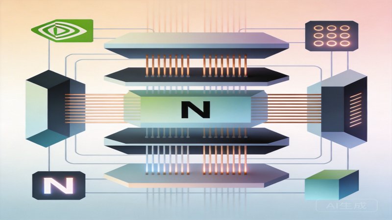
1. Architecture Layering
This report constructs a hypothetical layered architecture model for the Rubin platform, based on NVIDIA's emphasis on interconnect trends in the Blackwell architecture and industry focus on interconnect bottlenecks, to explore the potential challenges and changes brought by optical interconnect integration.
(PyTorch, TensorFlow)"] A2["CUDA/XLA Compiler & Runtime"] A3["Large-Scale Distributed Training Communication Library
(NCCL, potentially supporting optical interconnect primitives)"] A4["Performance Profiling & Debugging Tools"] end subgraph "System & Orchestration Layer" B1["GPU Cluster System Software Stack"] B2["NVLink/NVSwitch Drivers & Firmware"] B3["Optical Interconnect Link Management & Diagnostics Module"] B4["Resource Scheduler & Job Orchestrator
(e.g., Kubernetes Plugins)"] B5["Power & Thermal Management Controller"] end subgraph "Interconnect & Network Layer" C1["NVLink Optical Interconnect Links
(Intra-board/Inter-board)"] C2["NVLink Switch System
(potentially integrating optical switching)"] C3["Copper-Optical Hybrid Interconnect Architecture
(Transition Period)"] C4["Intra/Inter-Rack Optical Backplane/Fiber Cabling"] C5["System-Level Topology Management Unit"] end subgraph "Compute & Packaging Layer" D1["Rubin GPU/CPU Compute Cores"] D2["HBM/Other High-Speed Memory"] D3["NVLink Physical Layer Interface (Electrical/Optical)"] D4["Co-Packaged Optics (CPO) Engine
(Optional/Integrated)"] D5["Advanced Packaging Substrate (e.g., CoWoS)"] end A1 --> B1 A2 --> B1 A3 --> B1 B1 --> C5 B2 --> C2 B3 --> C1 B4 --> B5 C5 --> C1 C5 --> C2 C5 --> C3 C1 --> D3 C2 --> D3 D3 --> D4 D3 --> D1 D4 --> D5 D1 --> D5
Compute & Packaging Layer: This is the physical foundation for interconnects. Rubin compute cores connect to HBM and the NVLink physical layer interface via high-density interconnects. If the Rubin platform integrates CPO, it will be a key innovation. Its theoretical advantage lies in reducing electrical interconnect distance through advanced packaging, potentially lowering power consumption and signal loss, but specific benefits depend on the integration scheme and process maturity [Sources: TSMC & NVIDIA collaboration on advanced packaging, arXiv: Co-Packaged Optics (CPO) for AI Clusters].
Interconnect & Network Layer: This layer constructs the physical topology of the cluster. The core is the NVLink Optical Interconnect Link, used to replace copper cables for long-distance, high-bandwidth connections. The NVLink Switch System may integrate optical switching capabilities. Copper-Optical Hybrid Architecture serves as a transitional solution, intelligently allocating connection media based on distance and cost-effectiveness [Source: IEEE: Overview of Copper-Optical Hybrid Interconnect Architectures]. The system-level topology management unit is responsible for sensing and configuring the entire interconnect network.
System & Orchestration Layer: This layer is the software abstraction and management hub for hardware interconnect capabilities. NVLink/NVSwitch drivers and firmware need to support optical link initialization and error handling. The newly added Optical Interconnect Link Management and Diagnostics Module is responsible for monitoring optical signal quality (e.g., optical power, bit error rate) and performing dynamic adjustments. The resource scheduler can allocate tasks considering link status, and the thermal management controller must address new cooling challenges posed by CPO.
Application & Platform Layer: Upper-layer applications utilize interconnect capabilities through standard APIs (e.g., CUDA, NCCL), ideally agnostic to the underlying medium. However, future communication libraries like NCCL may introduce communication primitives optimized for the low latency and high bandwidth characteristics of optical interconnects to further improve distributed training efficiency.
2. Key Technologies
2.1 NVLink Optical Interconnect Technology
- Problem Solved: Addresses the limitations of traditional copper cables at ultra-high bandwidths (TB/s class), such as restricted transmission distance (typically <1-2 meters), decreased energy efficiency, and system scaling bottlenecks caused by signal attenuation, crosstalk, and soaring power consumption [Source: NVIDIA Blackwell Platform Architecture White Paper].
- Core Principle: Near the GPU's NVLink controller, high-speed parallel electrical signals are modulated onto lasers of specific wavelengths (e.g., 1310nm or 1550nm) via silicon photonic modulators, converting them to optical signals. Optical signals are transmitted through single-mode or multi-mode fiber, then demodulated back into electrical signals by photodetectors at the receiving end. The core is leveraging photons' extremely low transmission loss (~0.2 dB/km), extremely high bandwidth, and immunity to electromagnetic interference to achieve low-latency, high-bandwidth connections at rack-scale and even data center scale.
- Measured Effects/Technical Inference: No specific data for the Rubin platform currently exists. Referencing industry research, for distances greater than 10 meters, advanced optical interconnect solutions may consume 30%-50% less energy than traditional copper cable solutions [Comprehensive inference based on arXiv: Co-Packaged Optics (CPO) for AI Clusters and other papers]. Blackwell's NVLink 5.0 bandwidth has reached 1.8TB/s, and Rubin's NVLink optical interconnect target bandwidth is expected to move towards several TB/s.
2.2 Co-Packaged Optics (CPO)
- Problem Solved: Addresses issues caused by the distance (typically >5 cm) between pluggable optical modules and the ASIC/GPU, including high signal integrity loss, high power consumption (SerDes driver power being a major component), and limited front-panel bandwidth density improvement. Aims to achieve ultimate energy efficiency and integration density for ultra-high-speed interconnects.
- Core Principle: Integrates optical engines (lasers, modulators, detectors, etc.) with the GPU/switch ASIC on the same package substrate (e.g., silicon interposer) using 2.5D/3D advanced packaging technology. Electrical interconnect distance is reduced from centimeter-scale to millimeter-scale, significantly lowering driver power consumption and transmission loss for high-speed I/O. CPO is the ideal physical form to achieve NVLink optical interconnect's ultra-high bandwidth density (>10 Tbps/mm²) and ultra-low power (<5 pJ/bit) goals [Source: arXiv: Co-Packaged Optics (CPO) for AI Clusters].
- Measured Effects/Technical Inference: Academic research indicates CPO can reduce interconnect power consumption by approximately 30%-50% compared to pluggable optical modules and increase bandwidth density by an order of magnitude [Source: arXiv: Co-Packaged Optics (CPO) for AI Clusters]. NVIDIA's deep collaboration with TSMC on advanced packaging like CoWoS provides manufacturing feasibility for CPO integration in the Rubin platform [Source: TSMC & NVIDIA collaboration on advanced packaging]. Despite severe challenges, the industry is exploring advanced thermal solutions like microchannel cold plates and integrated thermal vias (TSV) to address CPO's thermal management issues.
2.3 Copper-Optical Hybrid Interconnect Architecture
- Problem Solved: During the transition period when optical interconnects (especially CPO) are costly and technology is not fully mature, how to balance system performance, power consumption, cost, and engineering complexity to achieve a smooth evolution from all-copper to all-optical interconnects.
- Core Principle: A hierarchical design based on the trade-off principle of "distance-bandwidth-cost". Retains optimized ultra-short-reach copper interconnects (e.g., micro-bump interconnects based on advanced packaging) for scenarios requiring extremely short distances and high-density connections (e.g., within multi-chip modules on the same substrate, between GPUs on the same motherboard). Employs optical interconnects for intra-rack cross-node, inter-rack, or longer-distance connections. The system manages links of different media via hardware identification or software policies to achieve transparent or semi-transparent data routing [Source: IEEE: Overview of Copper-Optical Hybrid Interconnect Architectures].
- Technical Inference: In a hybrid architecture, the boundary for medium selection will be based on a comprehensive trade-off of multiple factors like distance, bandwidth requirements, cost, and signal integrity. For example, copper may still be used for extremely short-range, high-density connections, while optical interconnects are preferred for long-range, high-bandwidth connections. Its management mechanism may be implemented by NVSwitch firmware or system management units based on pre-configured topology tables and link capability discovery functions [Based on technical logic inference].
3. Principle & Process Flow
The following flowchart describes the core steps of a typical distributed AI training data exchange (e.g., an All-Reduce operation) in a hypothetical Rubin cluster with optical interconnects, focusing on data plane operations.
(with Optical Engine) participant Optical_Link as Optical Interconnect Physical Link participant Sys_Mgr as System Monitoring & Management Layer Note over App, Sys_Mgr: Step 1: Data Generation & Task Distribution App->>Runtime: Decompose computation graph, initiate All-Reduce communication request Runtime->>Runtime: Plan communication path (copper/optical) based on known cluster topology Note over App, Sys_Mgr: Step 2: Communication Request Trigger & Data Transmission Runtime->>NVLink_Ctrl: Submit data transfer request (source/destination address, data) NVLink_Ctrl->>NVLink_Ctrl: Electrical signal processing, encoding, serialization NVLink_Ctrl->>Optical_Link: Electro-Optic Conversion (E/O), transmit optical signal Optical_Link->>Optical_Link: Optical signal transmission in fiber Optical_Link->>NVLink_Ctrl: Opto-Electric Conversion (O/E), restore electrical signal NVLink_Ctrl->>NVLink_Ctrl: Deserialization, decoding, error checking NVLink_Ctrl-->>Runtime: Confirm transmission completion Note over App, Sys_Mgr: Step 3: System-Level Monitoring & Background Optimization loop Continuous Background Monitoring Optical_Link->>Sys_Mgr: Report link metrics (optical power, BER, temperature) NVLink_Ctrl->>Sys_Mgr: Report power consumption & performance counters Sys_Mgr->>Sys_Mgr: Analyze data, trigger maintenance or optimization policies
(e.g., adjust laser bias, update topology mapping) end
Process Details:
- Data Generation & Parallel Task Distribution: The AI framework decomposes the training task, and the system orchestrator allocates tasks and data to each Rubin GPU.
- GPU-to-GPU High-Speed Data Exchange Trigger & Data Transmission: This is the technical core. The NCCL runtime generates specific communication operations based on pre-configured or discovered topology information. The NVLink controller prepares data and executes the transfer. On paths using optical interconnects, high-speed electrical signals are modulated onto lasers at the source GPU's CPO engine or onboard optical module, transmitted via fiber to the target end, demodulated into electrical signals, and written into the target GPU's memory. The entire process is managed by hardware and low-level drivers, transparent to upper-layer software.
- System-Level Monitoring & Background Optimization: A dedicated optical link management module continuously monitors the health (optical power, BER) and performance of optical links. This is a background process that does not affect real-time data plane operations. The system can perform dynamic optimization based on monitoring data, for example: adjusting laser power based on link aging to maintain performance; or planning pre-maintenance alerts and traffic rerouting for degraded optical links.
4. Open Research Questions
- Specific technical specifications and implementation level of NVLink optical interconnect in the Rubin platform: Its specific wavelength, modulation format (e.g., PAM4/NRZ), per-lane rate, target aggregate bandwidth, and whether it adopts CPO integration or onboard/pluggable optical module form are all currently without official data, requiring subsequent product announcements or whitepaper disclosures.
- Specific demarcation boundaries and collaborative management mechanisms for copper-optical hybrid architecture: How do factors like distance, topology, and cost specifically influence medium selection? Is the judgment and switching logic hardware-hardened or flexibly configurable via software policies? This directly affects system flexibility and optimization potential.
- Thermal management challenges posed by CPO integration: CPO thermal management is severely challenging, stemming from laser threshold current and wavelength being extremely sensitive to temperature, while GPU core heat generation is massive and fluctuates intensely. Coordinated heat dissipation within advanced packaging requires solving thermal coupling and precise temperature control issues, likely relying on aggressive cooling solutions like microchannel liquid cooling, which directly impacts packaging complexity and cost [Based on analytical inference].
- Impact of optical interconnects on the NVLink protocol stack and system reliability: Optical link failure modes (e.g., laser failure, fiber break) differ from copper cables (e.g., signal attenuation). Does NVLink's flow control, error retransmission mechanism need adaptation? Does the system level require new redundant link design, fast failover, and optical layer diagnostic tools to ensure high availability?
- Cost Increment and Return on Investment (ROI) Model: Introducing optical interconnects (especially CPO) is expected to significantly increase material and manufacturing costs. Therefore, a clear ROI model must be built to quantify the performance gains and power reductions it brings to weigh against its high cost increment, convincing data center operators.
- Ecosystem Openness and Standards: Will NVIDIA's optical interconnect technology adopt industry open standards (e.g., UCIe-P, OIF's CPO-related standards) or establish a private technology system? This will determine the ease of access for third-party optical module, switch, and server vendors, thereby affecting the entire ecosystem's competitive landscape and costs.
5. Competitive Landscape Analysis
5.1 Main Competitors
| Competitor | Technology Path | Core Strengths | Core Weaknesses |
|---|---|---|---|
| AMD | Instinct MI300 Series & Beyond: Uses advanced packaging based on TSMC CoWoS, integrating CPU/GPU/HBM. Interconnect relies on Infinity Fabric, and actively develops Xilinx's silicon photonics technology. Emphasizes open ecosystem, supports industry standards (e.g., UCIe, CXL). | 1. Gains silicon photonics technology reserves through Xilinx acquisition, possessing photonic-electronic co-design capabilities. 2. Unified CPU+GPU memory architecture offers advantages in certain HPC/AI workloads. 3. Emphasis on open standards may gain broader server OEM support. | 1. Software ecosystem (ROCm) maturity and developer community scale still lag behind CUDA. 2. Infinity Fabric's demonstrated bandwidth and scale validation for hyperscale AI cluster interconnects has not yet reached NVLink's level. 3. Public progress in deep CPO integration with GPUs appears slightly slower than NVIDIA's. |
| Intel | Gaudi Series AI Accelerators & Next-Gen: Uses silicon photonics-based pluggable optical modules (e.g., 1.6T modules) for rack-scale interconnection. Also strongly promotes the UCIe (Universal Chiplet Interconnect) open standard, paving the way for future chiplet integration including optical engines. | 1. Possesses deep expertise in silicon photonics R&D and manufacturing, with optical module products already in mass production. 2. A major initiator and promoter of the UCIe alliance, holding a high ground in building an open chiplet ecosystem. 3. Has a complete product line from chips, interconnects to servers. | 1. Gaudi accelerators have a relatively small share and influence in the mainstream AI training market. 2. The popularity and model coverage breadth of its AI accelerator software stack (Habana) need improvement. 3. Current solutions still primarily rely on pluggable optical modules; public roadmaps for tight CPO integration with AI accelerator ASICs are less aggressive than NVIDIA's. |
| Cloud Vendor In-House Chips (e.g., Google TPU, AWS Trainium) | Custom ASIC + Dedicated Interconnect: E.g., TPU uses custom high-speed interconnect networks and deploys optical switching at scale. The path involves deep hardware-software co-optimization, customized for their own cloud workloads. | 1. Deep vertical integration of hardware and software enables extreme optimization and energy efficiency for specific workloads (e.g., Transformer). 2. Complete control over the entire stack from chip to data center allows rapid iterative innovation in interconnect tech. 3. No burden of selling chips externally, enabling adoption of more aggressive, costlier technologies (e.g., early large-scale optical switching deployment). | 1. Technology is confined within their own cloud platforms, not constituting direct competition in the general AI chip market. 2. Ecosystem is locked in; developers cannot use them on their own infrastructure, limiting flexibility. 3. Chip iteration is driven by a single company's internal needs, potentially lacking generality. |
5.2 Differentiation Positioning
The core differences between this approach (NVIDIA Rubin path) and competitors:- Full-Stack Vertical Integration & Ecosystem Lock-in Advantage: NVIDIA provides a complete closed-loop solution from GPU, NVLink interconnect, CPO technology, NVSwitch, to the CUDA software stack. This deep integration offers significant advantages in performance tuning and rapid feature rollout but also constitutes a strong ecosystem barrier. This contrasts sharply with the "open standards + multi-vendor" path promoted by AMD/Intel.
- Forward-Looking & Aggressive Nature of CPO Integration: Based on deep collaboration with TSMC, NVIDIA's public progress in integrating cutting-edge packaging interconnect technologies like CPO into its mainstream GPU roadmap (Blackwell -> Rubin) is the most open and aggressive. Its goal is to make optical interconnect a core feature, not a peripheral, directly addressing GPU scaling bottlenecks. Competitors currently emphasize pluggable optical modules or long-term chiplet visions more.
- NVLink-Centric Performance Benchmark: NVLink continues to set industry benchmarks for GPU-to-GPU interconnect bandwidth and latency (Blackwell reaches 1.8TB/s). Rubin's optical interconnect evolution will directly reinforce this advantage, aiming to support continued expansion of the "single logical GPU" scale. Competitors' interconnect technologies (e.g., Infinity Fabric) are either more focused on CPU-GPU communication or still have gaps in scale validation for pure AI accelerator clusters.
5.3 Competitive Landscape Assessment
- Current Market Structure: According to historical data such as TrendForce's Q4 2023 "Global AI Chip Market Report," NVIDIA holds a dominant share in the AI training chip market. AMD has made breakthroughs in some scenarios with MI300X, and Intel's Gaudi series shows cost advantages in specific inference scenarios, but both still have a significant gap compared to NVIDIA in overall ecosystem and market scale. Cloud vendor in-house chips form closed loops within their own cloud services.
- Trends in Structure Evolution: Short-term (2-3 years), NVIDIA's leading position is difficult to shake; successful optical interconnect integration in Rubin would further solidify its advantage in the high-performance cluster market. Medium to long term, competition will focus on: 1) Open ecosystems (UCIe, etc.) and their ability to weaken CUDA's lock-in; 2) Cost reduction and maturity of optical/electrical interconnect technologies, and who can achieve a breakthrough in cost-performance; 3) Specific scenarios (e.g., inference, edge AI) may provide differentiated opportunities for competitors. Hybrid architectures and multiple technology paths will coexist long-term.
6. Key Judgments (Simplified Summary)
| # | Core Judgment | Why It Matters | Actionable Insights |
|---|---|---|---|
| 1 | The Rubin platform will substantively introduce optical interconnects, but initial implementations will most likely appear in a "copper-optical hybrid" form, with CPO being a long-term goal or option for specific models. | This determines the future physical architecture, cost structure, and scalability ceiling of AI clusters. Hybrid architecture is key to balancing performance and commercial viability. | Data center operators should plan for next-generation racks with fiber cabling and high power density cooling capabilities. Investors can focus on companies in the silicon photonics and advanced packaging supply chain. |
| 2 | The primary value of optical interconnects will shift from "extending distance" to "improving energy efficiency and bandwidth density", supporting the scale expansion to tens of thousands of GPUs within a rack. | AI computing power growth is constrained by the "power wall"; interconnect energy efficiency becomes critical to overall system efficiency. Increasing bandwidth density is a prerequisite for increasing compute density. | Chip and system design teams need to treat "interconnect power/bit" as a core optimization metric equally important as compute power. |
| 3 | NVIDIA will continue to maintain its "closed but efficient" full-stack ecosystem, developing in parallel with the "open but fragmented" industry standard path, potentially leading to de facto private standards in the interconnect domain. | Ecosystem openness affects the competitive landscape, innovation speed, and customer cost across the entire supply chain. Private standards may offer performance advantages but increase vendor lock-in risk. | Enterprise customers need to evaluate the trade-off between vendor lock-in and performance advantages. Developers should monitor CUDA ecosystem progress while also understanding open alternatives like ROCm. |
| 4 | Thermal management is one of the most severe engineering challenges for CPO integration, potentially impacting initial product yield, reliability, and maximum power settings. | Laser performance is highly sensitive to temperature, and coupled heat dissipation design with high-temperature GPU heat sources is extremely complex. This is a key risk point for product launch timing and achieving expected performance. | Monitor progress by NVIDIA and partners in advanced cooling technologies like liquid cooling and microchannel cooling. Thermal solution providers will play a more critical role. |
| 5 | The cost increment of optical interconnects will be the biggest obstacle to their widespread adoption, likely limited to hyperscale data centers and high-end HPC systems in the early stages. | High costs directly impact end-users' Total Cost of Ownership (TCO) and Return on Investment (ROI), determining the technology penetration rate. | The industry chain needs to collaborate to reduce costs of silicon photonic chips, advanced packaging, and optical components. Users need to establish detailed TCO/ROI models to evaluate adoption timing. |
- High Confidence Judgments (e.g., Judgments 1, 3): Supported by clear official roadmap direction (Rubin emphasizing advanced interconnects) and long-observed NVIDIA business strategies.
- Medium Confidence Judgments (e.g., Judgments 2, 4, 5): Strong logical inferences based on physical principles (optical interconnect energy efficiency advantages), academic research (CPO thermal challenges), cost structure analysis, and general industry technology trends.
- Low Confidence Judgments: This report does not contain low-confidence judgments. Uncertainties regarding specific technical specifications, cost data, and other undisclosed information are listed as open questions in the relevant section.
Why it Matters
Technology Positioning: Ecosystem Expansion: Integrating optical interconnect into the core moat through full-stack vertical integration.
Competitive Moat: Strengthens the full-stack moat via NVLink optical interconnect and CPO foresight, deepening ecosystem lock-in.
Industry Stage: Peak of Inflated Expectations
DECISION
For Vendor (NVIDIA)
- Accelerate engineering validation of CPO-GPU integration and clarify the commercial path for hybrid architecture.
- Pre-research optical-interconnect-aware communication primitives in CUDA/NCCL to solidify software advantage.
Strategic Moves: Publish Rubin platform interconnect whitepaper to clarify the technology roadmap.
For Enterprise (Enterprises using high-end AI clusters (e.g., cloud providers, AI companies, large enterprise tech departments))
- Assess data center fiber cabling and high-density liquid cooling capabilities in preparation for optical upgrades.
- Develop a refined TCO/ROI model incorporating interconnect power and bandwidth density.
Adoption Strategy: Fast Follower
For Investor
- Focus on companies in the silicon photonics, advanced packaging (CoWoS), and high-speed connector supply chain.
- Be wary of the risk that high optical interconnect costs may slow market penetration.
Key Risk: CPO thermal management and high cost may delay product commercialization and adoption.
PREDICT
1 year (High confidence)
NVIDIA will clarify the Rubin interconnect scheme, likely demonstrating a copper-optical hybrid prototype.
2 years (Medium confidence)
High-end AI servers begin widespread support for on-board optical engines, with CPO only piloted in top-tier systems.
3 years+ (Medium confidence)
Optical interconnect costs begin to decline, becoming a standard option for hyperscale data center expansion.
Get 3-5 key AI infrastructure signals weekly →
💬 Comments (0)