I. Event Review: Milestone Moments in AI Chip Supply Chain
July 1, 2026, marked a concentrated window of significant announcements across the global semiconductor industry. Multiple heavyweight developments converged simultaneously, sketching the contours of a profound restructuring underway in the AI chip supply chain. On this day, capital markets and industry participants alike felt the strong pulse emanating from twin engines: advanced process nodes and high-bandwidth memory.
In the memory domain, Samsung Electronics officially confirmed that the yield of its HBM4E (5th-generation high-bandwidth memory) had breached the critical 70% threshold. This breakthrough carries symbolic significance. HBM4E is manufactured using Samsung's D1d DRAM process, representing one of the industry's most advanced memory technologies. Samsung plans to pass PRA (Product Reliability Assessment) in November this year, meaning HBM4E will be qualified for large-scale commercial shipment before the end of 2026. The yield climb from approximately 45% at the beginning of the year to over 70% took Samsung less than two quarters, outpacing market expectations. For AI chip design giants such as NVIDIA and AMD, the HBM supply bottleneck that has constrained GPU shipments may finally see meaningful relief.
Simultaneously, Samsung unveiled its long-term logic process roadmap: SF1.4 (equivalent to 1.4nm) is slated for mass production in 2029, while the even more advanced SF1.4+ is planned for 2030. To support this roadmap, Samsung has shared process plans with Applied Materials and Lam Research, and is importing High NA EUV (High Numerical Aperture Extreme Ultraviolet) lithography systems from ASML. These moves signal Samsung's intent to mount a frontal challenge to TSMC at nodes below 2nm.
Capital markets reacted violently. ASML shares surged 6.8% to reach all-time highs. The driving force came from Korea's memory duopoly—Samsung and SK Hynix collectively plan four new mega-fabs with total investment of 800 trillion KRW (approximately $580 billion USD), a substantial portion of which will flow to ASML for EUV and High NA EUV lithography systems. ASML, as the absolute monopolist in semiconductor lithography, is emerging as one of the biggest beneficiaries of this capacity expansion frenzy.
In the foundry sector, TSMC's performance was equally impressive. Its US-listed ADR jumped 5.26% on the day, with single-day trading volume reaching $6.65 billion—topping all US stocks. UBS promptly issued a research report raising TSMC's target price to NT$3,400 and explicitly predicting that TSMC would initiate price hikes for its N2P (2nd-generation 2nm) process in Q1 2027. This forecast is grounded in the persistent tightness of TSMC's 2nm capacity, with leading customers including Apple, Qualcomm, and NVIDIA having pre-locked their 2027 capacity allocations.
Intel's turnaround story continued to unfold. Over the past year, Intel shares have skyrocketed 459%, with forward price-to-earnings ratio reaching a staggering 143x. Bank of America set a $135 target price, with the core thesis being that Intel's Xeon 6 processors have secured the position of host CPU for NVIDIA's next-generation AI supercomputing platform, DGX Rubin NVL8. This means Intel has reclaimed a critical position in the AI data center ecosystem, no longer a bystander in the GPU era.
AMD chose to compete through advanced packaging. Its newly launched Versal Premium Gen 2 adopts MoP (Module-on-Package) packaging technology, integrating 32GB of LPDDR5X memory and reducing PCB area by 60% compared to conventional solutions. This innovation carries significant value for edge AI and embedded high-performance computing scenarios.
Finally, Qualcomm officially announced the Snapdragon 8 Elite Gen6—the world's first 2nm Android flagship mobile chip. Manufactured using TSMC's N2P process, it delivers a 30% improvement in transistor density and a 36% reduction in power consumption compared to its predecessor. Qualcomm's move marks the formal entry of mobile terminals into the 2nm era, with AI computing power set to penetrate smartphones at scale.
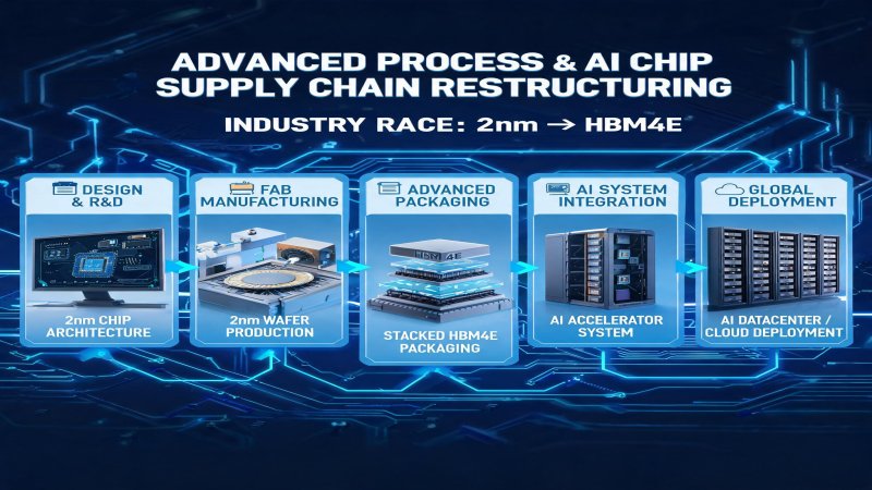
Taken together, the events of July 2026 are not isolated technology releases but a concentrated manifestation of systemic restructuring across the AI chip supply chain. From 2nm logic processes to HBM4E memory, from wafer foundries to advanced packaging, every link in the chain is undergoing profound transformation.
II. Technical Depth: The Architectural Revolution from 2nm to HBM4E
The technological evolution of advanced processes and HBM memory is fundamentally reshaping the physical foundation of AI chips. Understanding the depth of this transformation requires delving into every detail of transistor architecture, memory stacking, lithography technology, and packaging solutions.
2nm-Class Logic Processes: The Paradigm Shift from FinFET to GAA
The world's three leading foundries have adopted divergent technology roadmaps at the 2nm node. TSMC's N2/N2P processes continue using GAA (Gate-All-Around) transistor architecture, introducing a unique Nanosheet design that adjusts nanosheet width to balance performance and power. N2P, as the second-generation 2nm process, further optimizes transistor density and energy efficiency over N2, achieving approximately 310 million transistors per square millimeter—a roughly 30% improvement over the 3nm node. The Qualcomm Snapdragon 8 Elite Gen6 is among the first mass-production products on N2P, and its 36% power reduction validates this process's value in mobile applications.
Samsung's SF2 (2nm) family adopts MBCFET (Multi-Bridge-Channel FET) architecture, a specific implementation of GAA. Samsung's investment in GAA actually predates TSMC's, with technical differentiation primarily manifested in vertical channel control. According to Samsung's disclosed roadmap, SF1.4 (equivalent to 1.4nm) will enter mass production in 2029, with SF1.4+ following in 2030. To support this aggressive roadmap, Samsung has already imported High NA EUV equipment from ASML. The numerical aperture increases from 0.33 on conventional EUV to 0.55, improving resolution by approximately 70%. This means finer patterning can be achieved in a single exposure, dramatically reducing multi-patterning steps and thereby improving yield while lowering costs.
Intel, meanwhile, is pushing RibbonFET (a GAA variant) combined with PowerVia backside power delivery at its 20A (2nm-class) and 18A (1.8nm-class) nodes. Backside power delivery relocates power rails from the front to the back of the wafer, significantly reducing IR drop and signal crosstalk. Theoretically, this can improve frequency by 6% or reduce power consumption by 30%. Intel's Xeon 6 processors are manufactured on Intel 3 process, but the upcoming Xeon 7 series is planned for a full transition to 18A. Bank of America's optimism stems from the belief that if 18A achieves volume production on schedule in 2027, Intel can not only meet its own CPU requirements but potentially regain external foundry customers such as NVIDIA and Qualcomm.
HBM4E: A Leap in Memory Bandwidth
HBM4E delivers significant improvements over predecessor HBM4 in stack layers, per-die capacity, and data transfer rates. Samsung's HBM4E employs the D1d DRAM process, Samsung's 5th-generation 10nm-class DRAM technology, offering clear improvements in yield and performance over the previous D1a (4th-generation) process. The standard HBM4E stack comprises 16 layers with per-device capacity reaching 48GB and bandwidth exceeding 2TB/s. The yield breakthrough above 70% means Samsung can obtain sufficient qualified dies per 300mm wafer to control per-device HBM4E costs within an acceptable range.
Particular attention should be paid to HBM4E's interface standards. The HBM4 standard under development by JEDEC increases data bus width from 1024 bits on HBM3E to 2048 bits, meaning bandwidth doubles at the same frequency. Additionally, HBM4E introduces more advanced signal integrity solutions and on-die ECC (Error Correction Code) to meet AI training's demanding requirements for data reliability.
Four-Vendor Competitive Comparison Matrix
| Dimension | TSMC | Samsung | Intel | AMD |
|---|---|---|---|---|
| Most Advanced Process Node | N2P (2026 mass production) | SF2 (2025) / SF1.4 (2029) | 18A (2027 mass production) | Relies on foundry partners |
| Transistor Architecture | GAA Nanosheet | MBCFET (GAA) | RibbonFET + PowerVia | Depends on partner process |
| 2nm-Class Transistor Density | ~310MTr/mm² | ~300MTr/mm² | ~280MTr/mm² (18A target) | N/A |
| Key Customers | Apple, NVIDIA, Qualcomm, AMD | Samsung LSI, Qualcomm (partial), Tesla | Intel internal, potential external | Own chip designs |
| 2nm Capex (2025-2027) | ~$40B | ~$25B | ~$20B | No own fabs |
| HBM Product Line | None (foundry focus) | HBM4E (yield >70%) | None | Uses Samsung/SK Hynix HBM |
| Advanced Packaging | CoWoS, InFO, SoIC | I-Cube, X-Cube, HBM integration | Foveros, EMIB | MoP (Versal) |
| EUV Equipment Count (2026) | ~80 units | ~50 units | ~25 units | N/A |
| High NA EUV Adoption | Imports from 2028 | Confirmed import | Planned | N/A |
| Target Market Focus | HPC, Mobile, AI | Memory, Mobile, Foundry | Data Center, AI, Foundry | Data Center, Embedded, Gaming |
Advanced Packaging: The Underestimated Battlefield
As physical limits to process scaling increasingly constrain Moore's Law, advanced packaging has become the critical path for its continuation. TSMC's CoWoS (Chip-on-Wafer-on-Substrate) is central to NVIDIA's GPU+HBM integration solution and remains in severe supply shortage. Samsung's I-Cube and X-Cube families target the same market. AMD's MoP packaging represents a different philosophy—deeply integrating memory and logic dies at the packaging level to reduce PCB area and system power. The 60% PCB area reduction in Versal Premium Gen 2 means more compute nodes can be deployed per rack in data center and edge computing scenarios, with profound implications for total cost of ownership (TCO).
III. Financial Logic: The ROI Game Behind Trillion-Dollar Capex
The semiconductor industry has always been capital-intensive, but investment intensity at the 2nm-class advanced process and HBM4E level has reached unprecedented scale. Understanding this round of financial logic requires analysis across three dimensions: capital expenditure (Capex), revenue forecasts, and cost structures.
Capital Expenditure: The Scale and Structure of an Arms Race
TSMC's capital expenditure during 2025-2027 is projected to exceed $100 billion, with approximately 40% directed at 2nm and below advanced processes. A single 2nm fab costs $20-25 billion to build, roughly 1.5x that of a 5nm fab. The main drivers of cost inflation include: EUV lithography systems (each High NA EUV machine costs over $350 million), more complex cleanroom facilities, and expanded equipment counts due to increased process steps. A core pillar of UBS's TSMC target price upgrade to NT$3,400 is the judgment that TSMC's return on invested capital (ROIC) will continue improving—its pricing power allows it to pass a substantial portion of costs to customers.
Samsung is fighting on two fronts simultaneously—foundry and memory—making its capex scale even more massive. In 2026, Samsung Semiconductor's capital expenditure is projected to reach $35 billion, with approximately $10 billion directed at foundry 2nm/1.4nm capacity and $20 billion at memory expansion (including HBM4E and new fabs in Pyeongtaek and Yongin). The Korean government's announced 800 trillion KRW ($580 billion) K-Semiconductor Belt plan will construct four mega-fabs over the next decade, with Samsung and SK Hynix as primary investors. This scale is equivalent to approximately 1.5x the global semiconductor industry's annual capex, reflecting both commercial logic and profound national strategic considerations.
Intel's capex strategy carries a higher-risk bet character. Under CEO Pat Gelsinger's IDM 2.0 strategy, Intel plans to invest approximately $50 billion over four years in new fabs and process R&D. The US CHIPS and Science Act provides Intel with roughly $8 billion in direct subsidies and $11 billion in loan guarantees, partially alleviating financial pressure. However, Intel's current forward PE of 143x indicates that market expectations for future earnings have already priced in a very long growth cycle. Bank of America's $135 target price assumes that Intel regains external foundry customers through 18A by 2027 and restores data center revenue growth above 25% annually.
Revenue Forecasts: Who Benefits Most from 2nm and HBM4E?
From a foundry revenue perspective, TSMC's 2026 revenue is projected to reach $90-95 billion, with 2nm-related revenue share growing from approximately 5% in 2026 to over 25% by 2028. TSMC's N2P wafer prices are expected at $25,000-30,000 per wafer, more than double 5nm process pricing. High wafer prices combined with high capacity utilization (TSMC's advanced processes consistently run above 90%) form the cornerstone of its high gross margins. UBS's predicted 5-8% price hike in Q1 2027 would further push gross margins above 55%.
Samsung Foundry's 2026 revenue is projected at $15-18 billion. While only about one-fifth of TSMC's scale, its growth rate is faster (projected above 30% year-over-year). Samsung's strategy relies on more aggressive pricing (typically 15-20% below TSMC) to attract external customers, while leveraging synergies from its captive HBM and memory businesses. If SF2/SF1.4 processes can approach TSMC's performance and yield at equivalent nodes, Samsung could raise its foundry market share from approximately 12% currently to 18-20% by 2028-2029.
The HBM market's financial model is equally noteworthy. The 2026 global HBM market is projected at $35-40 billion, with HBM4E share growing from approximately 20% in 2026 to over 60% by 2028. Samsung's HBM4E yield breakthrough above 70% means its unit costs will decline approximately 25% compared to early HBM4 production, directly improving Samsung Memory's profitability. However, as SK Hynix and Micron catch up on HBM4E, average selling prices (ASP) will face downward pressure in 2027. We forecast HBM4E quarterly ASP may decline 8-12% between Q4 2026 and Q2 2027, but volume growth will offset price erosion, keeping total revenue growth above 20% annually.
Cost Analysis: The True Manufacturing Cost of 2nm Chips
A smartphone SoC manufactured on N2P process (such as Qualcomm Snapdragon 8 Elite Gen6) incurs foundry costs of approximately $80-100 per die, nearly double the $40-50 on 5nm nodes. This means wafer processing accounts for an increasing share of flagship mobile chip BOM (bill of materials)—from approximately 15% currently to over 25%. Qualcomm can pass these costs to OEMs (Samsung, Xiaomi, OPPO), but whether OEMs pass price increases to consumers depends on premium smartphone market competition dynamics.
For AI data center chips, cost structures are more complex. A single NVIDIA B200 or Rubin-architecture GPU incurs foundry costs of approximately $300-400, HBM4E memory costs of $800-1,200, and advanced packaging (CoWoS) costs of $200-300. Combined manufacturing costs approach $2,000 per die, while NVIDIA's selling prices remain $20,000-30,000, maintaining gross margins above 80%. This means even if TSMC and Samsung raise prices, NVIDIA has ample margin to absorb cost increases. However, for cloud service providers (AWS, Azure, Google Cloud), if GPU prices climb further due to foundry and memory price hikes, their return on capital will be squeezed, potentially dampening demand.
IV. Strategic Depth: Three-Way Competition and Geopolitical Games
Competition in advanced processes and AI chips has never been purely technical or financial. It is deeply intertwined with national strategy, supply chain security, and geopolitics. The industrial landscape in 2026 is evolving from TSMC's superpower dominance toward a three-way contest, with geographic factors playing an increasingly important role.
Competitive Landscape: The Triangular Game of TSMC, Samsung, and Intel
TSMC currently commands approximately 62% of the global advanced process market (5nm and below) and enjoys near-monopoly status at the 2nm node. Its core competitiveness lies in unmatched yield control (N3E yield already exceeds 80%), a vast customer ecosystem (virtually all top-ten global chip design houses are customers), and deep engineering talent reserves. TSMC's copy strategy—simultaneously building capacity in Hsinchu, Taichung, Kaohsiung, Arizona (USA), Kumamoto (Japan), and Dresden (Germany)—further cements its hub position in the global semiconductor supply chain.
However, TSMC's challenges are accumulating. Primary among them is geopolitical risk. Tensions across the Taiwan Strait make TSMC's capacity concentration (approximately 90% of advanced processes in Taiwan) a global supply chain single point of failure. The US government continues pressuring TSMC to shift more advanced capacity to its Arizona fab. Although TSMC has committed to building two 2nm fabs in Arizona (targeting 2028 production start), costs (US fab construction costs roughly 30% above Taiwan) and talent shortages remain unresolved.
Samsung represents TSMC's most credible challenger. Its absolute dominance in memory (ranked first globally in DRAM and NAND Flash) provides unique synergies for its foundry business—customers can obtain one-stop service encompassing logic foundry, HBM memory, and advanced packaging. Samsung intensified its offensive in 2026: securing HBM4E supply advantage through D1d process leadership, while demonstrating long-term logic process commitment through its SF1.4/SF1.4+ roadmap. Samsung has also adopted an open strategy, sharing process plans with Applied Materials and Lam Research. This ecosystem co-building approach helps accelerate process maturity and equipment matching.
Intel's role is the most peculiar. As a former technology leader, Intel's delays at the 10nm node cost it five years of leadership. But IDM 2.0 investments and the 18A process roadmap show its fight to the death determination. Intel Xeon 6 securing the host CPU position in NVIDIA DGX Rubin NVL8 represents Intel's most important design win in AI in recent years. This means not only revenue (projected $2-3 billion annual incremental data center CPU revenue) but more importantly validates Intel's capabilities in advanced packaging and system-level design. If 18A achieves volume production on schedule in 2027, Intel could become the third advanced process supplier after TSMC and Samsung.
Geopolitical Factors: The Chip War Enters a New Phase
US export controls on China have tightened progressively through 2025-2026, restricting not only advanced AI chip exports (such as NVIDIA H20/B20) to China but also attempting through long-arm jurisdiction to limit ASML and Applied Materials' service capabilities for Chinese customers. The direct consequence is that China's semiconductor industry is forced to accelerate localization, while the global supply chain faces further fragmentation risk.
For mainland China, SMIC's most advanced volume production process remains N+2 (equivalent to 7nm). While competitive in mature processes (28nm and above), the gap with TSMC and Samsung in advanced processes remains over five years. Huawei Kirin chips' continued iteration (reportedly using equivalent 5nm process) demonstrates China's capability for technological breakthrough under constraints, but mass production and high yields remain enormous challenges.
For Korea, US-China technology decoupling presents both opportunity and risk. The opportunity lies in Korean memory and foundry industries becoming objects of courtship for both superpowers. The risk: if the US demands Korea join advanced equipment export controls against China, Samsung and SK Hynix's massive investments in China (Xi'an, Dalian, Wuxi) would face operational difficulties. The Korean government's 800 trillion KRW K-Semiconductor Belt plan partly aims to reduce dependence on Chinese capacity and enhance domestic supply chain resilience.
Europe and Japan are also actively positioning. The EU Chips Act plans EUR 43 billion to boost local capacity, but primarily focuses on mature processes and automotive chips. Japan's Rapidus project aims for 2nm breakthroughs, but funding and technical reserves appear insufficient to change the landscape in the near term.
Supply Chain Restructuring: From Globalization to Regionalization
Over the past three decades, the semiconductor supply chain was built on globalized division of labor: US design, Taiwan manufacturing, Korea memory, China packaging, Japan materials. But this model is evolving toward regionalized clusters: the US (Arizona, Texas), Taiwan, and Korea (Pyeongtaek, Yongin) each forming complete advanced process ecosystems; mainland China building autonomous closed loops in mature processes and specific equipment/materials.
The direct cost of this restructuring is efficiency loss. According to Boston Consulting Group (BCG) estimates, fully regionalized semiconductor supply chains would raise global chip manufacturing costs by 15-25%. But for national governments, supply chain security has overtaken cost efficiency as the priority. ASML's record highs driven by Korea's four new fabs exemplify regionalization dividends—when every region seeks local capacity, equipment vendors become the biggest beneficiaries.
V. Challenges and Concerns: The Risk Matrix Behind the Celebration
Despite capital markets' extreme optimism about the semiconductor super-cycle (TSMC's $6.65 billion single-day turnover, Intel's 459% annual surge, ASML's all-time highs), multiple risks lurk beneath the surface. For investors and industry decision-makers, identifying these risks and crafting responses is essential.
Technical Risks: Physical Limits Below 2nm and Yield Traps
The 2nm node is widely regarded as the last mainstream generation of silicon-based CMOS processes. As transistor channel lengths shrink below 2nm, quantum tunneling, leakage current, and short-channel effects deteriorate sharply, causing power control difficulty to rise exponentially. While TSMC's N2P process mitigates some issues through GAA architecture, sustaining 15-20% annual performance improvement is becoming increasingly difficult.
Samsung faces even steeper challenges. SF2 process yields are reportedly still hovering around 60%, trailing TSMC N2's 75%+. Each 1 percentage point yield improvement, for a fab producing 30,000 wafers monthly, means tens of millions of dollars in additional annual profit. Samsung's SF1.4 targets 2029 mass production, but raising yields from current levels to commercially viable 80%+ within four years requires solving a complex array of materials, equipment, and process parameter optimization issues. High NA EUV improves resolution but also dramatically increases optical system complexity; equipment uptime and reticle costs remain unknowns.
Intel's 18A risk centers on PowerVia maturity. Backside power delivery is Intel's core differentiation, but the technology involves wafer thinning, backside via etching, and bonding—any misstep could cause yield collapse. Intel already suffered delays with its Intel 20A process in 2024-2025, and market trust in its execution capabilities has not fully recovered. If 18A is delayed again, Intel's foundry revival faces serious setbacks.
HBM4E technical risks concentrate on stacking and thermal management. Vertical stacking of 16 DRAM dies imposes extreme demands on TSV (Through-Silicon Via) yield and heat dissipation. Samsung's yield breakthrough above 70% is encouraging, but reaching HBM3E-era 85%+ yields will require another 6-12 months of continuous optimization. Furthermore, HBM4E power density rises approximately 20% over predecessor generations. In high-heat environments like GPUs, thermal design becomes a system-level bottleneck.
Cyclical Risks: Demand Bubbles and Inventory Corrections
The semiconductor industry is highly cyclical, and whether the AI computing investment boom is approaching a bubble threshold is a question investors must confront. In 2025-2026, global cloud service providers increased AI infrastructure capex by over 40% year-over-year, with Microsoft, Amazon, Google, and Meta collectively spending over $200 billion annually on AI-related infrastructure. But can this investment pace be sustained?
Historical experience shows that every new technology (3G, 4G, cloud computing) has experienced a cycle of over-investment—overcapacity—price collapse—consolidation. While AI computing demand is real (large model training and inference genuinely require massive GPU deployment), current investment rhythms may be running ahead of actual application monetization. If AI application commercialization returns fall short of expectations in 2027, cloud providers could rapidly cut capex, triggering GPU and HBM inventory corrections.
Intel's forward PE of 143x is a dangerous signal. Even if Xeon 6 wins NVIDIA adoption and 18A achieves volume production, raising earnings to match this valuation within two to three years is extremely challenging. Once market sentiment turns, the drawdown magnitude for high-valuation growth stocks is often devastating. TSMC and ASML valuations appear more reasonable (forward PE of 22x and 35x respectively), but neither would be immune if the industry enters a down-cycle.
Geopolitical Risks: Taiwan Strait and US-China Decoupling Tail Risks
Among all risks, geopolitical risks carry low probability but maximum potential impact. Taiwan produces approximately 90% of global advanced process chips and 65% of HBM memory. Any event affecting TSMC's normal operations—whether natural disaster, geopolitical conflict, or political intervention—would inflict nuclear winter level shock on global technology industries. Even non-war scenarios, such as stricter US export controls on Taiwan or mainland China imposing enhanced economic sanctions, could significantly disrupt supply chains.
Deepening US-China technology decoupling is another key variable. If the US expands semiconductor controls against China during 2026-2027 (for example, restricting maintenance services for 14nm-and-below equipment, or prohibiting third-party exports containing US technology to China), global supply chains face even more severe fragmentation. For Samsung and SK Hynix, which operate fabs in China, this means dramatically increased operational complexity and compliance costs.
Korea's tightrope walking between the US and China also carries risk. If the US pressures Korea to join advanced memory export controls against China, Samsung and SK Hynix would face a painful choice between their China market (approximately 30% of memory revenue) and US subsidies/technology cooperation.
VI. Conclusion: Forward-Looking Judgments from an Investment Perspective
At the July 2026 juncture, the restructuring of advanced processes and AI chip supply chains is accelerating. 2nm processes are moving from laboratories to mass production; HBM4E is transitioning from supply bottleneck to volume shipment; the competitive landscape is evolving from TSMC dominance toward multi-polar competition. For investors and industry participants, this historic transformation harbors enormous opportunities alongside non-negligible risks.
Investment Perspective: Core Assets and Risk-Return Profiles
From a risk-return perspective, TSMC remains the most certain core asset in the advanced process race. The technical leadership of its N2P process, customer stickiness, and pricing power constitute deep moats. UBS's NT$3,400 target price (corresponding to 2027 forward PE of approximately 25x) appears reasonable within a growth stock framework. TSMC's primary risk is geopolitical, but its diversified global capacity footprint (Taiwan, USA, Japan, Germany) is gradually reducing this concentration risk. For long-term investors, TSMC should be a priority accumulation target on any pullback driven by macro or geopolitical factors.
ASML, as the absolute monopolist in semiconductor equipment, embodies the ultimate pick-and-shovel investment logic. Whether TSMC, Samsung, or Intel compete at nodes below 2nm, all must purchase EUV and High NA EUV equipment from ASML. Korea's 800 trillion KRW expansion plan means ASML's order visibility extends beyond 2030. While its current 35x forward PE is not cheap, its technology monopoly and long-term growth certainty still warrant portfolio allocation.
Samsung represents a potential dark horse in this cycle. If HBM4E yields continue improving and Samsung captures more NVIDIA GPU配套 share in 2027, its memory business profitability will significantly improve. Meanwhile, SF1.4/SF1.4+ roadmap execution could unlock valuation premium for its foundry business. Samsung's current valuation (forward PE around 12x) shows significant discount to TSMC, a discount that could narrow if geopolitical risks ease and foundry business breaks through.
Intel is a high-risk, high-reward turnaround play. The past year's 459% surge has priced in substantial optimism, but 143x forward PE means any execution stumble could trigger violent correction. For investors capable of tolerating high volatility, Intel retains upside on catalysts such as 18A process qualification and external foundry customer wins. For risk-averse investors, current levels warrant a wait-and-see approach.
Forward-Looking Judgments: Key Nodes Over the Next Three Years
Looking ahead, the following milestones will determine industry trajectory:
First, November 2026: Samsung HBM4E PRA certification. This will be the starting gun for large-scale HBM4E shipments, directly impacting AI GPU supply and pricing in H1 2027. If certification proceeds smoothly, the HBM market will shift from seller's market toward balance, and cloud providers' AI infrastructure costs could decline 10-15%.
Second, Q1 2027: TSMC N2P price increases. This event will test TSMC's pricing power at 2nm and downstream customers' (especially Apple and Qualcomm) acceptance. If price hikes stick and capacity utilization remains above 90%, TSMC gross margins will breach 55%, further widening profitability gaps with competitors.
Third, H2 2027: Intel 18A volume production. This is the ultimate test of Intel's IDM 2.0 strategy. If 18A yields reach 75%+ and Intel secures at least one external major customer (such as NVIDIA or Qualcomm), Intel formally returns to the advanced process first tier, and its valuation framework will shift from cyclical to growth.
Fourth, 2028-2029: Samsung SF1.4 mass production. If Samsung can achieve yields approaching TSMC's equivalent node at 1.4nm, the global advanced process market could evolve from one superpower, two strong powers to two-power rivalry, with TSMC share potentially declining from 62% to around 55%. While unfavorable for TSMC, this benefits overall industry health through enhanced competition and cost optimization.
Final Assessment
The industry race from 2nm to HBM4E is, in essence, the concentrated expression of global technological hegemony competition within semiconductors. One trillion dollars in capital expenditure, three competing technology roadmaps, and deep geopolitical engagement together constitute the grandest industrial narrative of our era. For investors, holding core assets (TSMC, ASML) while tactically allocating high-beta names (Samsung, Intel) represents the optimal strategy for navigating this transformation. For industry decision-makers, securing critical capacity, diversifying supply chains, and pre-positioning for next-generation technologies (High NA EUV, GAA transistors, advanced packaging) will determine competitive positioning over the next five years.
In this race from 2nm to HBM4E, there are no spectators—only participants and those left behind.
Why it Matters
The race in advanced processes and HBM memory directly determines the cost structure and supply capacity of AI computing infrastructure. TSMC's single-day turnover of $6.65 billion, Intel's 459% annual surge, and ASML's record highs demonstrate capital markets' extreme optimism about the semiconductor super-cycle. Samsung's HBM4E yield breakthrough above 70% signals potential easing of supply bottlenecks for AI server core components, while Qualcomm's 2nm flagship chip marks a new era for mobile AI computing. From an investment perspective, this supply chain restructuring involves over $1 trillion in planned capital expenditure and represents the core variable determining global tech industry dynamics over the next five years.
DECISION
Institutional investors: Increase core positions in TSMC and ASML. TSMC's Q1 2027 price hike expectations are clear with a target price range of NT$3,000-3,400; ASML benefits from Korea's 800 trillion KRW expansion plan with High NA EUV order visibility extending to 2030. Recommended allocation: TSMC 15%-20%, ASML 8%-10%.
Technology procurement decision-makers: Immediately secure long-term HBM4E orders. Samsung's D1d process leadership and November PRA approval will significantly ramp supply in H1 2027; simultaneously evaluate Intel Xeon 6 as an alternative host CPU for DGX Rubin NVL8 to diversify supply chain risks.
Semiconductor equipment and materials suppliers: Focus on Samsung SF1.4/SF1.4+ process collaboration opportunities. Applied Materials and Lam Research have been invited to participate; prepare High NA EUV supporting materials and inspection solutions in advance.
Risk-hedging investors: Intel's forward PE of 143x already fully reflects optimistic expectations. Consider tail-risk protection through put options or reduced positions; simultaneously monitor geopolitical factors impacting China-Korea-US semiconductor trade.
PREDICT
Q4 2026: Samsung HBM4E passes PRA certification and begins large-scale shipments to NVIDIA and AMD, putting downward pressure on HBM market prices with an expected quarterly average price decline of 8%-12%.
Q1 2027: TSMC initiates N2P process price increases of 5%-8%. Apple A19 Pro and Qualcomm Snapdragon 8 Elite Gen6 become the first large-scale mass-production customers, with 2nm wafer monthly capacity exceeding 50,000 wafers.
H2 2027: Intel Xeon 6 processor adoption in NVIDIA DGX Rubin NVL8 platforms reaches over 40%, driving Intel's data center business revenue growth exceeding 35% year-over-year.
2029-2030: Samsung's SF1.4 mass production and SF1.4+ launch will reshape the advanced process triopoly. Market shares for TSMC, Samsung, and Intel at nodes below 2nm may evolve from the current 62%/25%/13% to 55%/30%/15%.
Get 3-5 key AI infrastructure signals weekly →
💬 Comments (0)